RL78/G10 CHAPTER 24 ELECTRICAL SPECIFICATIONS
R01UH0384EJ0311 Rev. 3.11 603
Dec 22, 2016
24.6.4 SPOR circuit characteristics
(T
A = −40 to +85°C, VSS = 0 V)
Parameter Symbol Conditions MIN. TYP. MAX. Unit
Detection
voltage
Power supply
voltage level
V
SPOR0 Power supply rise time 4.08 4.28 4.45 V
Power supply fall time 4.00 4.20 4.37 V
VSPOR1 Power supply rise time 2.76 2.90 3.02 V
Power supply fall time 2.70 2.84 2.96 V
VSPOR2 Power supply rise time 2.44 2.57 2.68 V
Power supply fall time 2.40 2.52 2.62 V
VSPOR3 Power supply rise time 2.05 2.16 2.25 V
Power supply fall time 2.00 2.11 2.20 V
Minimum pulse width
Note
TLSPW 300 µs
Note Time required for the reset operation by the SPOR when V
DD becomes under VSPOR.
Caution Set the detection voltage (V
SPOR) in the operating voltage range. The operating voltage range depends
on the setting of the user option byte (000C2H). The operating voltage range is as follows:
When the CPU operating frequency is from 1 MHz to 20 MHz: V
DD = 2.7 to 5.5 V
When the CPU operating frequency is from 1 MHz to 5 MHz: V
DD = 2.0 to 5.5 V
24.6.5 Power supply voltage rising slope characteristics
(T
A = −40 to +85°C, VSS = 0 V)
Parameter Symbol Conditions MIN. TYP. MAX. Unit
Power supply voltage rising slope SVDD 54 V/ms
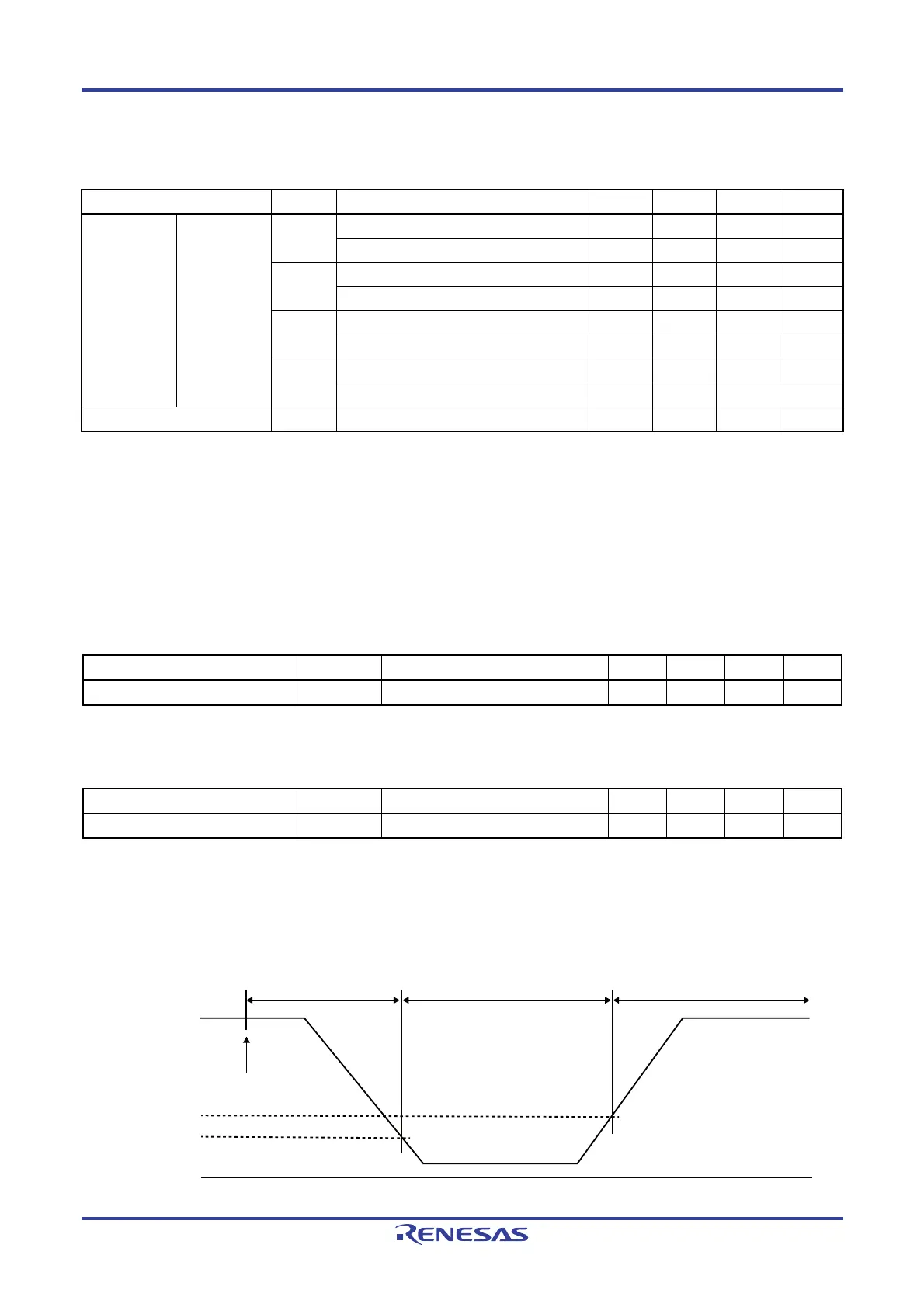
24.7 RAM Data Retention Characteristics
(T
A = −40 to +85°C, VSS = 0 V)
Parameter Symbol Conditions MIN. TYP. MAX. Unit
Data retention power supply voltage VDDDR 1.9 5.5 V
Caution Data in RAM is retained until the power supply voltage becomes under the minimum value of the data
retention power supply voltage (V
DDDR). Note that data in the RESF register might not be cleared even
if the power supply voltage becomes under the minimum value of the data retention power supply
voltage (V
DDDR).
STOP mode
STOP instruction
execution
SPOR reset period Normal operation
(Retain data in RAM and RESF)
V
DD
VDDDR
Rising of VSPOR
Falling of VSPDR

 Loading...