RL78/G10 CHAPTER 10 A/D CONVERTER
R01UH0384EJ0311 Rev. 3.11 258
Dec 22, 2016
10.7.2 Setting up A/D conversion of the internal reference voltage (16-pin products only)
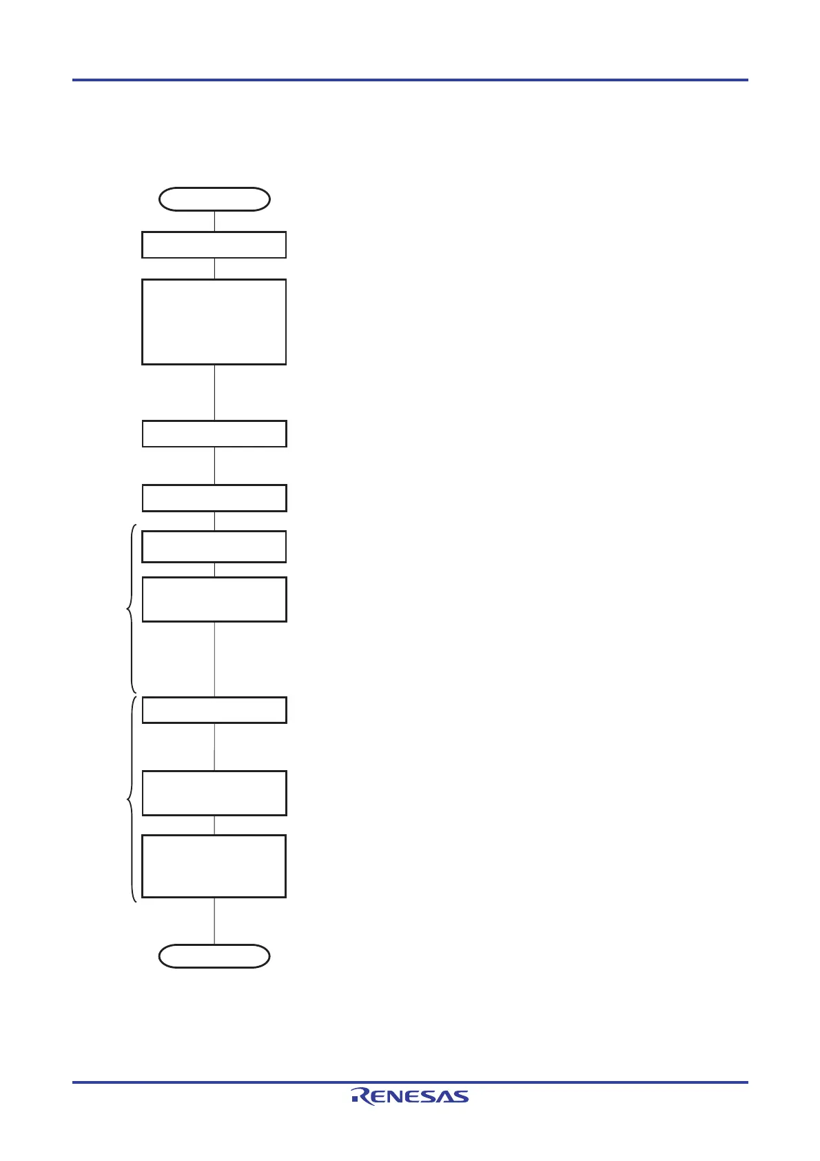
Figure 10-16. Setting Up A/D Conversion of Internal Reference Voltage
Start of setup
The ADCEN bit of the PER0 register is set (1), and a clock is provided to the A/D converter.
The conversion time and each mode of the A/D converter are set.
•
A/D converter mode register 0 (ADM0)
Clear LV0 bit to 0.
FR1 and FR0 bits: These bits are used to select the A/D conversion time.
•
A/D converter mode register 2 (ADM2)
ADTYP bit: This bit is used to select 10-bit or 8-bit resolution.
•
Analog input channel specification register (ADS)
Set ADS2, ADS1, ADS0 = 111B. Select the internal reference voltage (0.815 V (typ.))
as the target of A/D conversion.
The operation of the A/D voltage comparator is started.
•
The ADCE bit of the ADM0 register is set (1),
and the system enters the conversion standby status.
A/D conversion ends. The conversion result is stored in the ADCRH and ADCRL registers.
•
A/D conversion result higher-order bit storage register (ADCRH): Eight higher-order bits
•
A/D conversion result lower-order bit storage register (ADCRL): Two lower-order bits
At the same time, the A/D conversion end interrupt request signal (INTAD) is generated,
and the ADCS bit of the ADM0 register is automatically cleared (0) (conversion standby status).
After counting up to the stabilization wait time ends, the ADCS bit of the ADM0 register is
set (1) and discharging the sampling capacitor starts.
End
Setting PER0 register
•
Setting ADM0 register
•
Setting ADM2 register
•
Setting ADS register
(The order of the settings
is irrelevant.)
Setting ADCE bit
Setting ADTES register
End of A/D conversion
Storage of conversion results
in the ADCRH and ADCRL
registers
Setting ADCS bit
Start of discharging
A/D voltage stabilization
wait time count
Select V
SS as the target of A/D conversion to perform conversion with discharge
of the sampling capacitor.
•
The ADTES1 bit of the ADTES register is set (1).
Setting ADTES register
After discharging ends, the target of A/D conversion
is changed to the internal reference voltage (0.815 V (typ.)).
•
The ADTES1 bit of the ADTES register is cleared (0).
The ADCS bit of the ADM0 register is set (1) and A/D conversion starts.
Setting ADCS bit
Start of A/D conversion
End of A/D
conversion
At the same time, the A/D conversion end interrupt request signal (INTAD) is generated,
and the ADCS bit of the ADM0 register is automatically cleared (0) (conversion standby status).
First A/D
conversion
Second
and
subsequent
rounds of
/D
conversion
The stabilization wait time (0.1
µ
s) is counted by the software.

 Loading...