RL78/G10 CHAPTER 10 A/D CONVERTER
R01UH0384EJ0311 Rev. 3.11 256
Dec 22, 2016
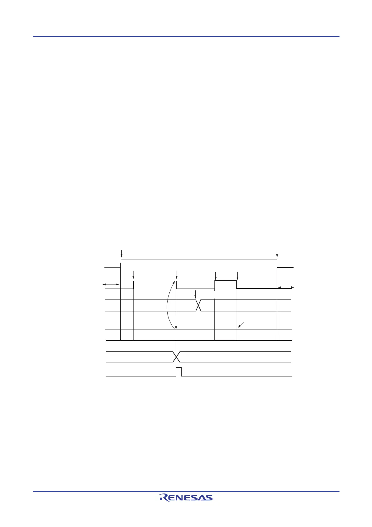
10.6 A/D Converter Operation Modes
The operation of the A/D converter is described below. In addition, the setting procedure is described in 10.7 A/D
Converter Setup Flowchart.
<1> In the conversion stop status, the ADCE bit of A/D converter mode register 0 (ADM0) is set to 1, and the system
enters the conversion standby status.
<2> After the software counts up to the stabilization wait time (0.1
μ
s), the ADCS bit of the ADM0 register is set to 1 to
start the A/D conversion of the analog input specified by the analog input channel specification register (ADS).
<3> When A/D conversion ends, the conversion result is stored in the A/D conversion result register (ADCRH,
ADCRL), and the A/D conversion end interrupt request signal (INTAD) is generated.
<4> After A/D conversion ends, the ADCS bit is automatically cleared to 0, and the system enters the conversion
standby status.
<5> When ADCS is cleared to 0 during conversion operation, the current A/D conversion is interrupted, and the
system enters the conversion standby status.
<6> When ADCE is cleared to 0 while in the A/D conversion standby status, the A/D converter enters the conversion
stop status. Setting ADCS =1 and ADCE = 0 is prohibited. Specifying 1 for ADCS in the conversion stopped
status (ADCS =0, ADCE = 0) is ignored and A/D conversion does not start.
Figure 10-14. Example of Operation Timing
ADCE
ADCS
ADS
INTAD
ADCRH,
ADCRL
A/D
conversion
status
ADCE is set to 1.
<1>
ADCS is set to
1 while in the
conversion
standby status.
ADCS is
automatically
cleared to
0 after
conversion
ends.
<2> <4>
<2>
A/D
conversion
ends.
<3>
Conversion is
interrupted.
ADCE is cleared to 0.
<6>
ADCS is
cleared to
0 during A/D
conversion
operation.
<5>
The trigger
is not
acknowledged.
The trigger
is not
acknowledged.
Conversion
standby
Conversion
standby
Conversion
standby
Data 0
(ANI0)
Stop
status
Data 0
(ANI0)
Data 0
(ANI0)
Data 1
(ANI1)
Data 1
(ANI1)
Stop
status
ADS is rewritten
(from ANI0 to ANI1).

 Loading...