RL78/G10 CHAPTER 8 CLOCK OUTPUT/BUZZER OUTPUT CONTROLLER
R01UH0384EJ0311 Rev. 3.11 230
Dec 22, 2016
CHAPTER 8 CLOCK OUTPUT/BUZZER OUTPUT CONTROLLER
8.1 Functions of Clock Output/Buzzer Output Controller
The clock output controller is intended for clock output for supply to peripheral ICs.
Buzzer output is a function to output a square wave of buzzer frequency.
One pin can be used to output a clock or buzzer sound.
The PCLBUZ0 pin outputs a clock selected by clock output select register 0 (CKS0).
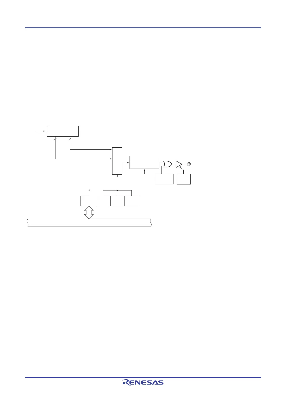
Figure 8-1 shows the block diagram of clock output/buzzer output controller.
Figure 8-1. Block Diagram of Clock Output/Buzzer Output Controller
fMAIN
PCLOE0
5
3
Clock/buzzer
controller
Prescaler
Selector
Internal bus
PCLOE0
Clock output select register 0 (CKS0)
CCS02 CCS00
PM02
(PM40)
Output latch
P02 (P40)
fMAIN/2
11
to fMAIN/2
13
fMAIN to fMAIN/2
4
CCS01
P02/ANI1/SCK00/SCL00/PCLBUZ0/KR3/
VCOUT0 (16-pin products)
(P40/KR0/TOOL0/(PCLBUZ0)/(TI01/TO01))
Caution For the frequency the PCLBUZ0 pin can output, refer to 24.4 AC Characteristics.
Remark Functions in parentheses in the above figure can be assigned via settings in the peripheral I/O redirection
register (PIOR).

 Loading...