RL78/G10 CHAPTER 13 SERIAL INTERFACE IICA
R01UH0384EJ0311 Rev. 3.11 412
Dec 22, 2016
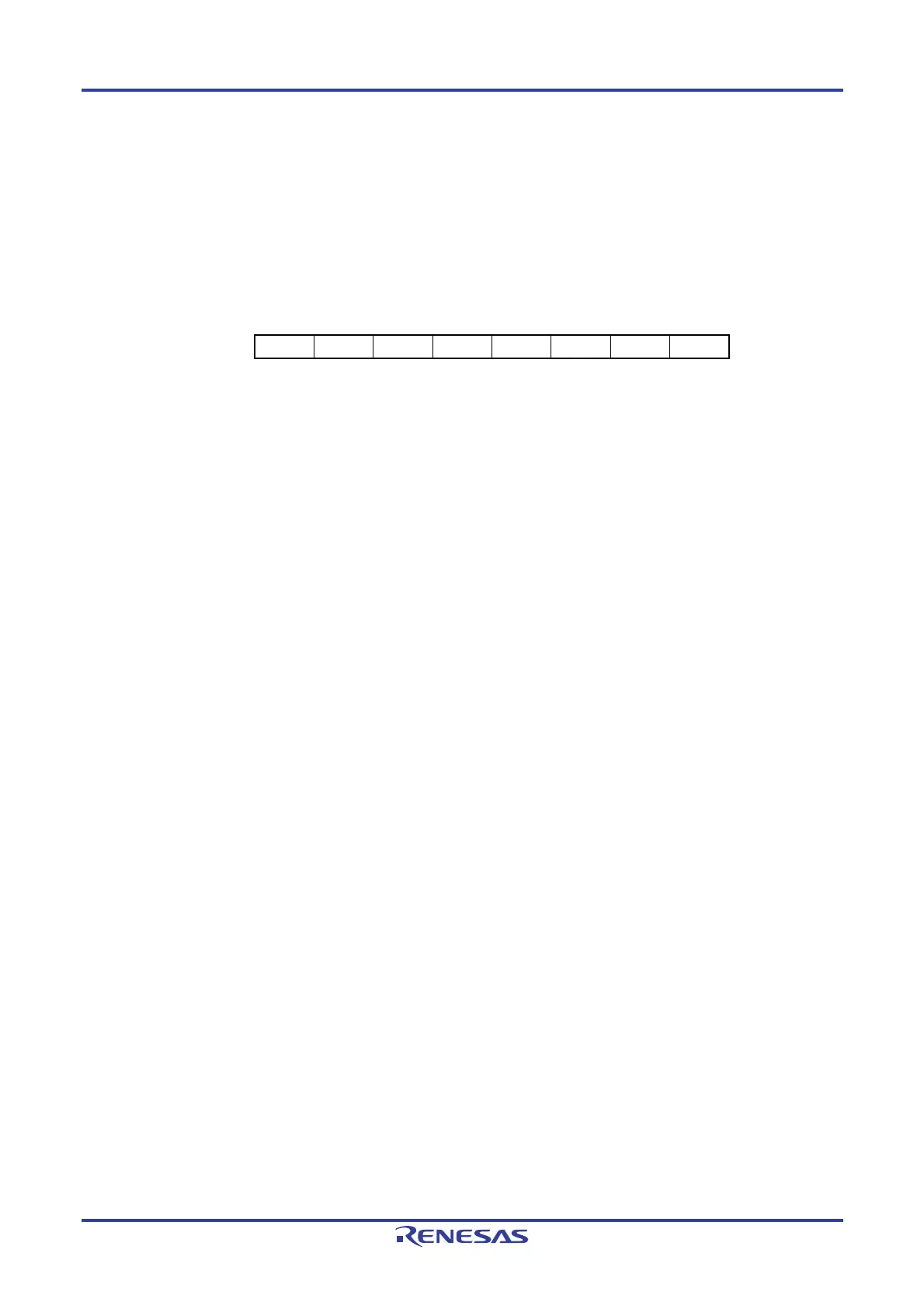
(2) Slave address register 0 (SVA0)
This register stores seven bits of local addresses {A6, A5, A4, A3, A2, A1, A0} when in slave mode.
The SVA0 register can be set by an 8-bit memory manipulation instruction.
However, rewriting to this register is prohibited while STD0 = 1 (while the start condition is detected).
Reset signal generation clears the SVA0 register to 00H.
Figure 13-4. Format of Slave Address Register 0 (SVA0)
Symbol
SVA0
Address: F0234H After reset: 00H R/W
76543210
0
Note
A0A1A2A3A4A5A6
Note Be sure to clear the bit 0 to 0.
(3) SO latch
The SO latch is used to retain the SDAA0 pin’s output level.
(4) Wakeup controller
This circuit generates an interrupt request (INTIICA0) when the address received by this register matches the
address value set to the slave address register 0 (SVA0) or when an extension code is received.
(5) Serial clock counter
This counter counts the serial clocks that are output or input during transmit/receive operations and is used to verify
that 8-bit data was transmitted or received.
(6) Interrupt request signal generator
This circuit controls the generation of interrupt request signals (INTIICA0).
An I
2
C interrupt request is generated by the following two triggers.
• Falling edge of eighth or ninth clock of the serial clock (set by the WTIM0 bit)
• Interrupt request generated when a stop condition is detected (set by the SPIE0 bit)
Remark WTIM0 bit: Bit 3 of IICA control register 00 (IICCTL00)
SPIE0 bit: Bit 4 of IICA control register 00 (IICCTL00)
(7) Serial clock controller
In master mode, this circuit generates the clock output via the SCLA0 pin from a sampling clock.
(8) Serial clock wait controller
This circuit controls the wait timing.
(9) ACK generator, stop condition detector, start condition detector, and ACK detector
These circuits generate and detect each status.
(10) Data hold time correction circuit
This circuit generates the hold time for data corresponding to the falling edge of the serial clock.

 Loading...