RL78/G10 CHAPTER 24 ELECTRICAL SPECIFICATIONS
R01UH0384EJ0311 Rev. 3.11 597
Dec 22, 2016
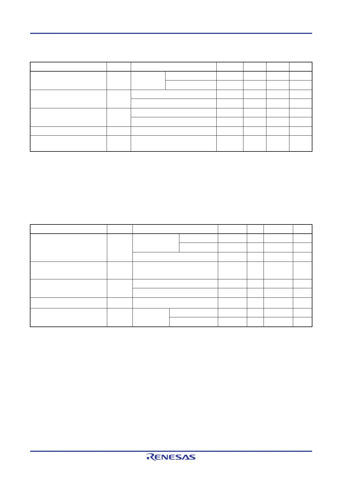
(2) CSI mode (master mode, SCKp... internal clock output)
(TA = −40 to +85°C, 2.0 V ≤ VDD ≤ 5.5 V, VSS = 0 V)
Parameter Symbol Conditions MIN. TYP. MAX. Unit
SCKp cycle time tKCY1 tKCY1 ≥ 4/fCLK 2.7 V ≤ VDD ≤ 5.5 V 200
ns
2.0 V ≤ VDD ≤ 5.5 V 800 ns
SCKp high-/low-level width tKH1, tKL1 2.7 V ≤ VDD ≤ 5.5 V
t
KCY1
/2 - 18
ns
2.0 V ≤ VDD ≤ 5.5 V
t
KCY1
/2 - 50
ns
SIp setup time (to SCKp↑)
Note 1
tSIK1 2.7 V ≤ VDD ≤ 5.5 V 47 ns
2.0 V ≤ VDD ≤ 5.5 V 110 ns
SIp hold time (from SCKp↑)
Note 1
tKSI1 19 ns
Delay time from SCKp↓ to SOp
output
Note 2
t
KSO1 C = 30 pF
Note 3
25 ns
Notes 1. When DAP0n = 0 and CKP0n = 0, or DAP0n = 1 and CKP0n = 1. The SIp setup time becomes “to SCKp↓” and
SIp hold time becomes “from SCKp↓” when DAP0n = 0 and CKP0n = 1, or DAP0n = 1 and CKP0n = 0.
2. When DAP0n = 0 and CKP0n = 0, or DAP0n = 1 and CKP0n = 1. The delay time to SOp output becomes “from
SCKp↑” when DAP0n = 0 and CKP0n = 1, or DAP0n = 1 and CKP0n = 0.
3. C is the load capacitance of the SCKp and SOp output lines.
(3) CSI mode (slave mode, SCKp... external clock input)
(T
A = −40 to +85°C, 2.0 V ≤ VDD ≤ 5.5 V, VSS = 0 V)
Parameter Symbol Conditions MIN. TYP. MAX. Unit
SCKp cycle time tKCY2 2.7 V ≤ VDD ≤ 5.5 V fMCK > 16 MHz 8/fMCK ns
fMCK ≤ 16 MHz 6/fMCK ns
2.0 V ≤ VDD ≤ 5.5 V 6/fMCK ns
SCKp high-/low-level width tKH2,
t
KL2
2.0 V ≤ V
DD ≤ 5.5 V tKCY2/
2 - 18
ns
SIp setup time (to SCKp↑)
Note 1
tSIK2 2.7 V ≤ VDD ≤ 5.5 V 1/fMCK + 20 ns
2.0 V ≤ VDD ≤ 5.5 V 1/fMCK + 30 ns
SIp hold time (from SCKp↑)
Note 1
tKSI2 2.0 V ≤ VDD ≤ 5.5 V 1/fMCK + 31 ns
Delay time from SCKp↓ to SOp
output
Note 2
t
KSO2 C = 30 pF
Note 3
2.7 V ≤ VDD ≤ 5.5 V 2/fMCK + 50 ns
2.0 V ≤ VDD ≤ 5.5 V 2/fMCK + 110 ns
Notes 1. When DAP0n = 0 and CKP0n = 0, or DAP0n = 1 and CKP0n = 1. The SIp setup time becomes “to SCKp↓” and
the SIp hold time becomes “from SCKp↓” when DAP0n = 0 and CKP0n = 1, or DAP0n = 1 and CKP0n = 0.
2. When DAP0n = 0 and CKP0n = 0, or DAP0n = 1 and CKP0n = 1. The delay time to SOp output becomes “from
SCKp↑” when DAP0n = 0 and CKP0n = 1, or DAP0n = 1 and CKP0n = 0.
3. C is the load capacitance of the SOp output lines.
Remarks 1. p: CSI number (p = 00, 01), n: Channel number (n = 0, 1)
2. f
MCK: Serial array unit operation clock frequency
(Operation clock to be set by the serial clock select register 0 (SPS0) and the CKS0n bit of the serial mode
register 0nH (SMR0nH). n: Channel number (n = 0, 1))

 Loading...


