RL78/G13 CHAPTER 20 POWER-ON-RESET CIRCUIT
R01UH0146EJ0100 Rev.1.00 883
Sep 22, 2011
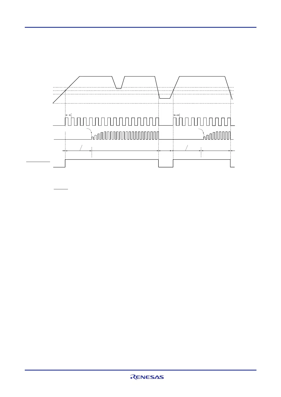
Figure 20-2. Timing of Generation of Internal Reset Signal by Power-on-reset Circuit
and Voltage Detector (1/2)
(1) When LVD is OFF (option byte 000C1H/010C1H: VPOC2 = 1B)
High-speed on-chip
oscillator clock (f
IH
)
High-speed
system clock (f
MX
)
(when X1 oscillation
is selected)
Starting oscillation is
specified by software
Operation
stops
Supply voltage
(V
DD
)
1.6 V
Note 1
Wait for oscillation
accuracy stabilization
Note 2
Wait for oscillation
accuracy stabilization
Note 2
Normal operation
(high-speed on-chip
oscillator clock)
Note 3
Normal operation
(high-speed on-chip
oscillator clock)
Note 3
Operation stops
Reset
period
(oscillation
stop)
Reset processing
Note 4
Reset processing
Internal reset signal
V
PDR
=
1.50 V (TYP.)
V
POR
=
1.51 V (TYP.)
CPU
0 V
Starting oscillation is
specified by software
Notes 1. The operation guaranteed range is 1.6 V ≤ VDD ≤ 5.5 V. To make the state at lower than 1.6 V reset state
when the supply voltage falls, use the reset function of the voltage detector, or input the low level to the
RESET pin.
2. The internal reset processing time includes the oscillation accuracy stabilization time of the high-speed on-
chip oscillator clock.
3. The high-speed on-chip oscillator clock and a high-speed system clock or subsystem clock can be selected
as the CPU clock. To use the X1 clock, use the oscillation stabilization time counter status register (OSTC)
to confirm the lapse of the oscillation stabilization time. To use the XT1 clock, use the timer function for
confirmation of the lapse of the stabilization time.
4. Reset processing time: 155 to 407
μ
s
Remark V
POR: POR power supply rise detection voltage
V
PDR: POR power supply fall detection voltage
<R>
<R>

 Loading...


