RL78/G13 CHAPTER 20 POWER-ON-RESET CIRCUIT
R01UH0146EJ0100 Rev.1.00 884
Sep 22, 2011
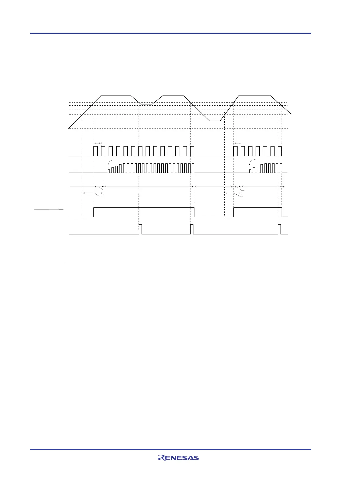
Figure 20-2. Timing of Generation of Internal Reset Signal by Power-on-reset Circuit
and Voltage Detector (2/2)
(2) When LVD is interrupt & reset mode (option byte 000C1/010C1H: LVIMDS1, LVIMDS0 = 1, 0)
High-speed on-chip
oscillator clock (f
IH
)
High-speed
system clock (f
MX
)
(when X1 oscillation
is selected)
Operation
stops
Supply voltage
(V
DD
)
1.6 V
Note 1
Wait for oscillation
accuracy stabilization
Note 3
Wait for oscillation
accuracy stabilization
Note 3
Normal operation
(high-speed on-chip
oscillator clock)
Note 2
Normal operation
(high-speed on-chip
oscillator clock)
Note 2
Operation stops
Reset
period
(oscillation
stop)
POR processing time
Internal reset signal
V
PDR
= 1.50 V (TYP.)
V
LVIH
V
POR
= 1.51 V (TYP.)
CPU
INTLVI
0 V
V
LVIL
Note 4
Starting oscillation is
specified by software
Starting oscillation is
specified by software
Reset processing time
POR processing time
Reset processing time
Note 5
Notes 1. The operation guaranteed range is 1.6 V ≤ VDD ≤ 5.5 V. To make the state at lower than 1.6 V reset state
when the supply voltage falls, use the reset function of the voltage detector, or input the low level to the
RESET pin.
2. The high-speed on-chip oscillator clock and a high-speed system clock or subsystem clock can be selected
as the CPU clock. To use the X1 clock, use the oscillation stabilization time counter status register (OSTC)
to confirm the lapse of the oscillation stabilization time. To use the XT1 clock, use the timer function for
confirmation of the lapse of the stabilization time.
3. The internal reset processing time includes the oscillation accuracy stabilization time of the high-speed on-
chip oscillator clock.
4. After the first interrupt request signal (INTLVI) is generated, the LVIL and LVIMD bits of the voltage
detection level register (LVIS) are automatically set to 1. If the operating voltage returns to 1.6 V or higher
without falling below the voltage detection level (V
LVIL), after INTLVI is generated, perform the required
backup processing, and then use software to specify the following settings in order:
<1> Clear the LVILV bit of the LVIS register to 0.
<2> Clear the LVIMD bit of the LVIS register to 0.
5. Reset processing time: 387 to 720
μ
s
Remark V
LVIH, VLVIL: LVD detection voltage
V
POR: POR power supply rise detection voltage
V
PDR: POR power supply fall detection voltage
<R>
<R>

 Loading...


