14
1
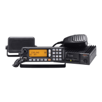
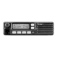
PANEL DESCRIPTION
1
2
3
4
5
6
7
8
9
10
11
12
13
14
15
16
17
18
19
20
21
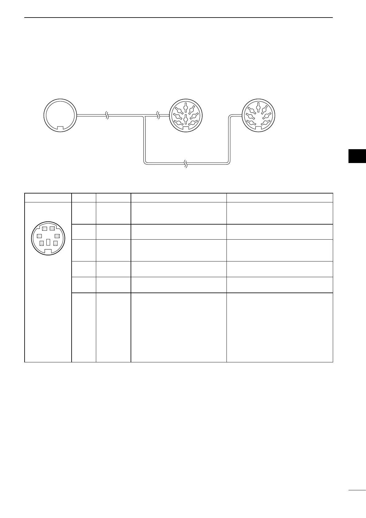
D DATA2 socket information
DATA2
PIN No.
NAME DESCRIPTION SPECIFICATIONS
Rear panel view
1
DATA IN
Input terminal for data transmit.
( 1200 bps: AFSK/
9600 bps: G3RUH, GMSK)
Input level (1200 bps)
Input level (9600 bps)
: 100 mV
: 0.2 to 0.5 Vp-p
2 GND
Common ground for DATA IN, DATA
OUT and AF OUT.
———
3
PTTP
PTT terminal for packet operation.
Connect to ground to activate the
transmitter.
Input voltage (High)
Input voltage (Low)
: 2.0 V to 20.0 V
: –0.5 V to +0.8 V
4
DATA OUT*
Data out terminal for 9600 bps op-
eration only.
Output impedance
Output level
: 10 k˘
: 1.0 Vp-p
5
AF OUT*
Data out terminal for 1200 bps op-
eration only.
Output impedance
Output level
: 4.7 k˘
: 100–300 mV rms
6
SQL*
Squelch out terminal. This pin is
grounded when the transceiver re-
ceives a signal which opens the
squelch.
•To avoid interferingtransmissions,
connect squelch to the TNC to inhibit
transmission when squelch is open.
•KeepRFgainatanormallevel,oth-
erwise a “SQL” signal will not be out-
put.
SQL open
SQL closed
: Less than 0.3 V/
5 mA
: More than 6.0 V/
100 µA
* The pin 4 (DATA), pin 5 (AF) and pin 6 (SQL) output capabilities are for the MAIN Band’s AF and squelch by de-
fault.Youcanchangethissettingin“DATAAF/SQLSelect”oftheSetmode.(p.166)
8
1
2
3
4
7
6
5
1
2
3
4
7
6
5
qwer
tyui
o!0!1!2
!3
Connect to ACC socket ACC 1 ACC 2
q FSKK
w GND
e HSEND
r MOD
t AF
y SQLS
u 13.8 V
i ALC
q 8 V
w GND
e HSEND
r BAND
t ALC
y VSEND
u 13.8 V
• When connecting the ACC conversion cable (OPC-599)
 Loading...