RL78/G10 CHAPTER 6 TIMER ARRAY UNIT
R01UH0384EJ0311 Rev. 3.11 161
Dec 22, 2016
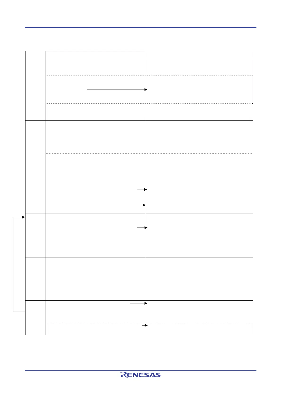
Figure 6-43. Procedure for Operating Interval Timer/Outputting Square Wave (1/2)
Software Operation Hardware Status
TAU
default
setting
Power-off status
(Clock supply is stopped and writing to SFR of the TAU is
disabled.)
Sets the TAU0EN bit of peripheral enable register 0
(PER0) to 1 (when the TAU0EN bit is 0, read/write
operation is disabled).
Power-on status. Each channel stops operating.
(Clock supply is started and writing to SFR of the TAU is
enabled.)
Sets timer clock select register 0 (TPS0).
Determines operating clock (CK00 and CK01) for each
channel.
Channel
default
setting
Sets timer mode register 0n (TMR0n) (determines
operation mode for each channel).
Sets interval (period) value in the timer data register 0n
(TDR0n) (for the access procedure to the TDR0nH and
TDR0nL registers, see 6.2.2 Timer data register 0n
(TDR0n)).
Channel stops operating.
Clears the target bit of timer output mode register 0
(TOM0) to 0 (master channel output mode).
Clears the target bit of the TOL0 register to 0.
To use square wave output:
Sets the TO0n bit and determines default level of the
TO0n output.
Sets the TOE0n bit to 1 and enables operation of
TO0n.
Clears the port register and port mode register to 0
(output mode is set).
The TO0n pin goes into Hi-Z state.
(The port mode register is set to input mode.)
TO0n does not change because channel stops operating (the
TO0n pin is not affected even if the TO0n bit is modified).
The level set in the TO0n bit is output from the TO0n pin.
Operation
start
Sets the TOE0n bit to 1 and enables operation of TO0n
(only if resuming square wave output operation).
Sets the target bit of TS0 or TSH0 register to 1.
The target bit of TS0 or TSH0 register automatically
returns to 0 because it is a trigger bit.
The target bit of TE0 or TEH0 register is set to 1, and count
operation starts.
Value of the TDR0n register is loaded to timer count
register 0n (TCR0n) at the next count clock. INTTM0n is
generated and TO0n performs toggle operation if the
MD0n0 bit of the TMR0nL register is 1.
During
operation
The set value of the TDR0n register can be changed.
The TCR0n register can always be read (for the access
procedure to the TCR0nH and TCR0nL registers, see
6.2.1 Timer counter register 0n (TCR0n)).
The set values in the target bits of the TO0 and TOE0
register can be changed.
The set values in the target bits of the TMR0n, TOM0,
and TOL0 registers cannot be changed.
Counter (TCR0n) counts down. When count value reaches
0000H, the value of the TDR0n register is loaded to the
TCR0n register again and the count operation is continued.
By detecting TCR0n = 0000H, INTTM0n is generated and
TO0n performs toggle operation.
After that, the above operation is repeated.
Operation
stop
Sets the target bit of TT0 or TTH0 register to 1.
The target bit of TT0 or TTH0 register automatically
returns to 0 because it is a trigger bit.
The target bit of the TE0 or TEH0 register is cleared to 0, and
count operation stops.
The TCR0n register holds count value and stops.
The TO0n output is not initialized but holds current status.
Clears the TOE0n bit to 0 and sets a value in the TO0n
bit.
The level set in the TO0n bit is output from the TO0n pin.
(Remark and Caution are listed on the next page.)
Operation is resumed.

 Loading...