6.5.1 INPUT MODULE CIRCUIT DESCRIPTION
V00239
Transformer
board
Serial
interface
Serial Link
Optical
Isolator
Noise
filter
Optical
Isolator
Noise
filter
Buffer
8 digital inputs
Parallel Bus
VT
or
CT
A/D Converter
VT
or
CT
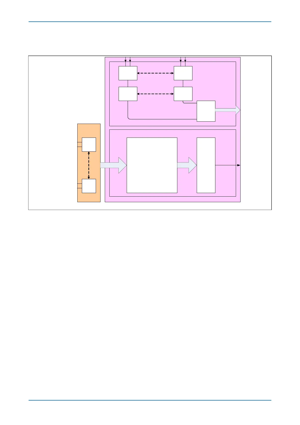
Figure 17: Input module schematic
A/D Conv
ersion
The differential analogue inputs from the CT and VT transformers are presented to the main input board as shown.
Each differential input is first converted to a single input quantity referenced to the input board’s earth potential.
The analogue inputs are sampled and converted to digital, then filtered to remove unwanted properties. The
samples are then passed through a serial interface module which outputs data on the serial sample data bus.
The calibration coefficients are stored in non-volatile memory. These are used by the processor board to correct
for any amplitude or phase errors introduced by the transformers and analogue circuitry.
Opto-isolated inputs
The other function of the input board is to read in the state of the digital inputs. As with the analogue inputs, the
digital inputs must be electrically isolated from the power system. This is achieved by means of the 8 on-board
optical isolators for connection of up to 8 digital signals. The digital signals are passed through an optional noise
filter before being buffered and presented to the unit’s processing boards in the form of a parallel data bus.
This selectable filtering allows the use of a pre-set filter of ½ cycle which renders the input immune to induced
power-system noise on the wiring. Although this method is secure it can be slow, particularly for inter-tripping. This
can be improved by switching off the ½ cycle filter, in which case one of the following methods to reduce ac noise
should be considered.
● Use double pole switching on the input
● Use screened twisted cable on the input circuit
The opto-isolated logic inputs can be configured for the nominal battery voltage of the circuit for which they are a
part, allowing different voltages for different circuits such as signalling and tripping.
P64x Chapter 3 - Hardware Design
P64x-TM-EN-1.3 47
 Loading...