(1)
Vector
address
Vector
address + 1
Vector
address + 2
Vector
address + 3
(2)
Internal processing
cycle
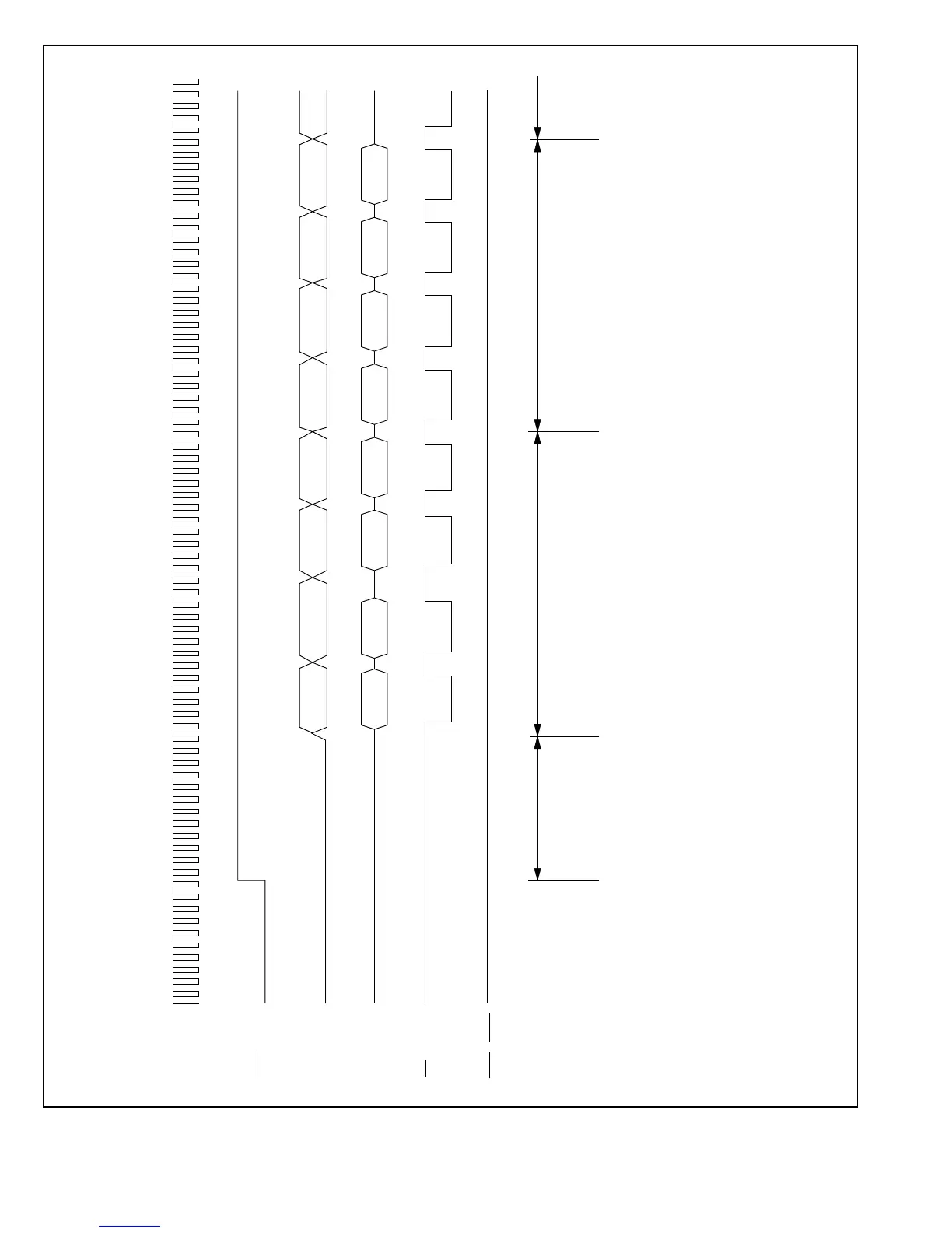
Note: This diagram applies to maximum mode when the program area and vector table are both in external memory.
After a reset, the wait-state controller inserts three wait states in each bus cycle.
(1) Program start address
(2) First instruction of program
Reset vector Prefetch first instruction of program Instruction
execution
cycle
ø
RES
RD
LWR, HWR
D to D
15 0
A to A23 0
don’t
care
Vector
CP
Vector
PC
Vector
PC
HL
Read signal
Write signal

 Loading...
