9.10 Port 9
9.10.1 Overview
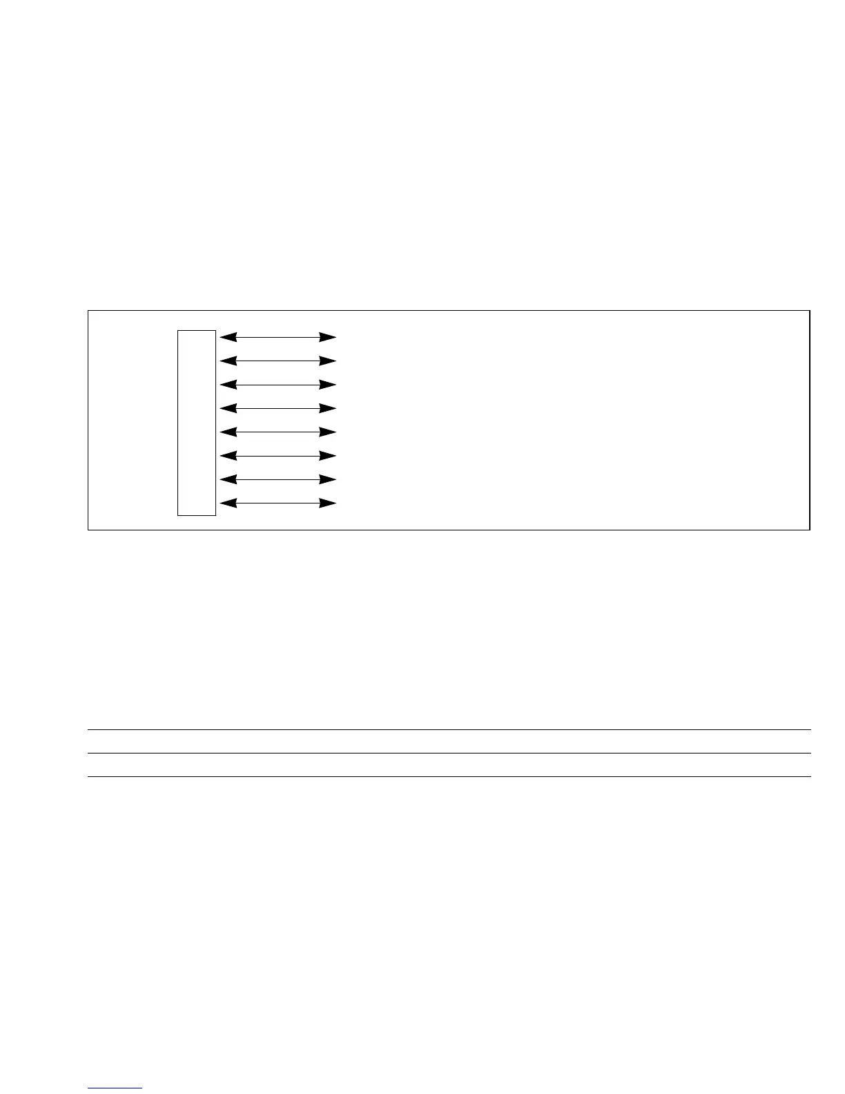
Port 9 is an 8-bit input/output port with the pin configuration shown in figure 9-21. In addition to
general-purpose input and output, its pins are used for the output compare A signals from free-
running timers 2 and 3, for PWM timer output, and for input and output by the on-chip serial
communication interface 9 (SCI). The pin functions are the same in all MCU operating modes.
Outputs from port 9 can drive one TTL load and a 30pF capacitive load. They can also drive a
Darlington transistor pair.
Figure 9-21 Pin Functions of Port 9
9.10.2 Port 9 Registers
Register Configuration: Table 9-15 lists the registers of port 9.
Table 9-15 Port 9 Registers
Name Abbreviation Read/Write Initial Value Address
Port 9 data direction register P9DDR W H'00 H'FFFE
Port 9 data register P9DR R/W H'00 H'FFFF
P97 (input/output) / SCK (input/output)
P9
6 (input/output) / RXD (input)
P9
5 (input/output) / TXD (output)
Port P9
4 (input/output) / PW3 (output)
9P9
3 (input/output) / PW2 (output)
P9
2 (input/output) / PW1 (output)
P9
1 (input/output) / FTOA3 (output)
P9
0 (input/output) / FTOA2 (output)
173
Downloaded from Elcodis.com electronic components distributor

 Loading...
