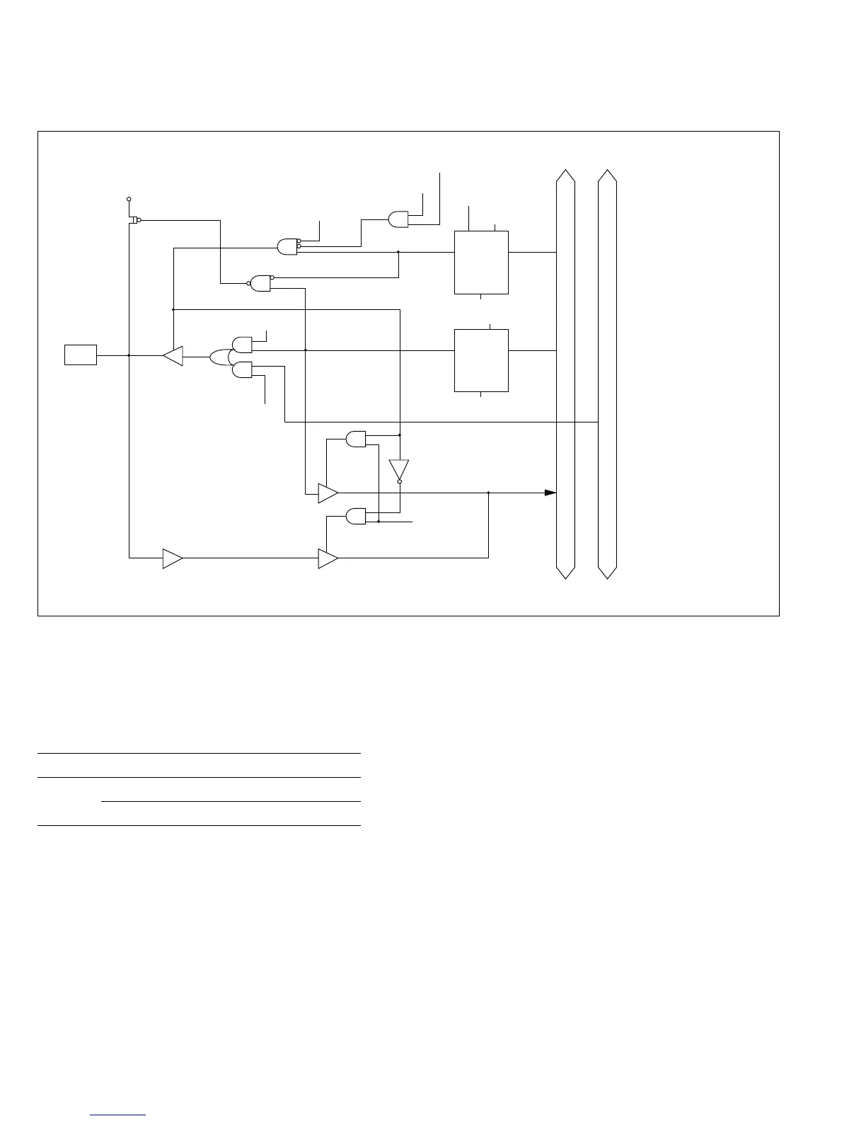
C.6 Schematic Diagram of Port 6
Figure C-6 gives a schematic view of the port 6 input/output circuits.
Table C-6 Port 6 Port Read
Mode Port Read Data
3 DR value
DDR = 0 Pin value
DDR = 1 DR value
WP6D:
WP6:
RP6:
n:
Write to P6DDR
Write to Port 6
Read Port 6
0 to 3
Internal data bus (PDB8 to PDB15)
Mode 3
Software standby
Bus release
Mode 1, 2, or 7
Mode 3 or 4
RP6
P6n
WP6
C
R
QD
P6 DR
n
C
R
QD
P6 DDR
n
Reset
WP6D
Reset
S
Internal address bus (IAB16 to IAB19)
MOS
pull-up
Mode 3 or 4
1,2,4,7
Figure C-6 Schematic Diagram of Port 6
417
Downloaded from Elcodis.com electronic components distributor

 Loading...
