RD, WR
R/W, DS
D –D
70
A –A19 0
ø
BREQ
BACK
(1) (2) (3) (4)
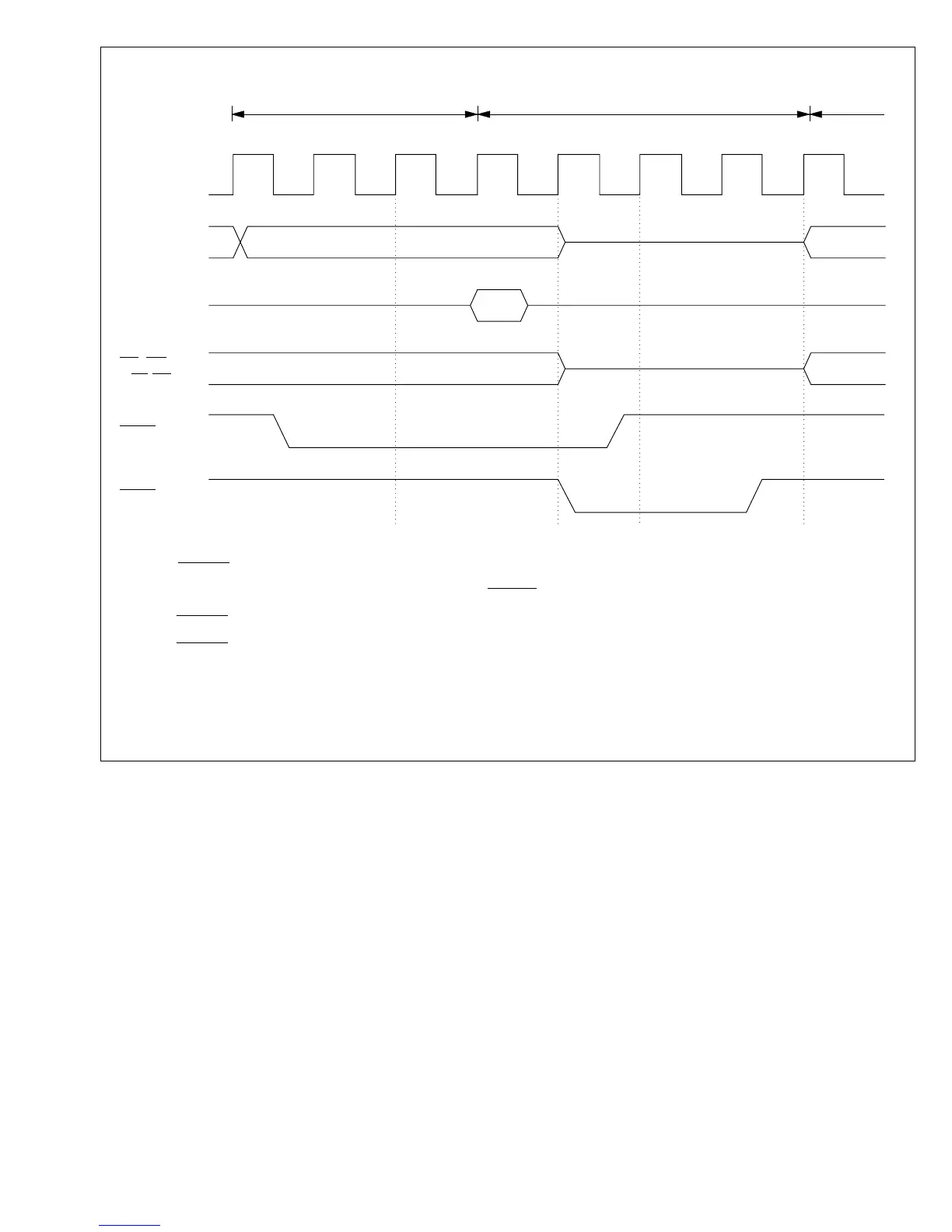
Fig. 3-14
Bus-right release cycle CPU cycleExternal access cycle
T
1 T2 TW TXT3 TX TX T1**
(1) The BREQ pin is sampled at the start of the TW state and the Low level is detected.
(2) At the end of the external access cycle, the BACK pin goes Low and the CPU releases the bus.
(3) The BREQ pin is sampled at the T
X state and a High level is detected.
(4) The BACK pin is returned to the High level, ending the bus-right release cycle.
* T
W : Wait state.
T
X : Bus-right released state.
Figure 3-14 Bus-Right Release Cycle (During External Access Cycle)
74
Downloaded from Elcodis.com electronic components distributor

 Loading...
