17.3 Programming
The write, verify, and inhibited sub-modes of the PROM mode are selected as shown in
table 17-4.
Table 17-4 Selection of Sub-Modes in PROM Mode
Pins
Mode CE OE V
PP VCC 07 to 00 A14 to A0
Write Low High VPP VCC Data input Address input
Verify High Low V
PP VCC Data output Address input
Programming inhibited High High V
PP VCC High-impedance Address input
Note: The V
PP and VCC pins must be held at the VPP and VCC voltage levels.
The H8/532 PROM uses the same, standard read/write specifications as the HN27C256 and
HN27256.
17.3.1 Writing and Verifying
An efficient, high-speed programming procedure can be used to write and verify PROM data.
This procedure writes data quickly without subjecting the chip to voltage stress and without
sacrificing data reliability. It leaves the data H'FF written in unused addresses.
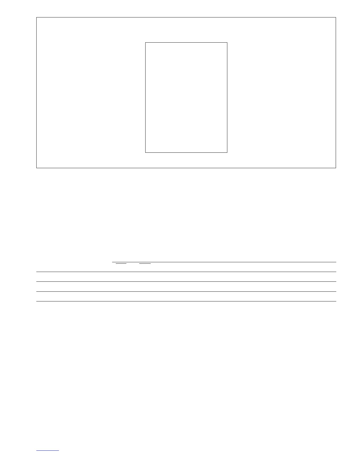
On-chip ROM
Address in MCU mode Address in PROM mode
H'0000 H'0000
H'7FFF H'7FFF
Figure 17-3 Memory Map in PROM Mode
299
Downloaded from Elcodis.com electronic components distributor

 Loading...
