Bit 2 Bit 1 Bit 0 Description
CKS2 CKS1 CKS0 Clock Source Overflow Interval (ø = 10MHz)
0 0 0 ø/2 51.2µs (Initial value)
0 0 1 ø/32 819.2µs
0 1 0 ø/64 1.6ms
0 1 1 ø/128 3.3ms
1 0 0 ø/256 6.6ms
1 0 1 ø/512 13.1ms
1 1 0 ø/2048 52.4ms
1 1 1 ø/4096 104.9ms
13.2.3 Notes on Register Access
The watchdog timer’s TCNT and TCSR registers differ from other registers in being more difficult
to write. The procedures for writing and reading these registers are given below.
1. Writing to TCNT and TCSR: These registers must be written by word access. Programs
cannot write to them by byte access. The word must contain the write data and a password.
The watchdog timer’s TCNT and TCSR registers both have the same write address. The write
data must be contained in the lower byte of the word written at this address. The upper byte
must contain H'5A (password for TCNT) or H'A5 (password for TCSR). See figure 13-2.
The result of the access depicted in figure 13-2 is to transfer the write data from the lower byte
to the TCNT or TCSR.
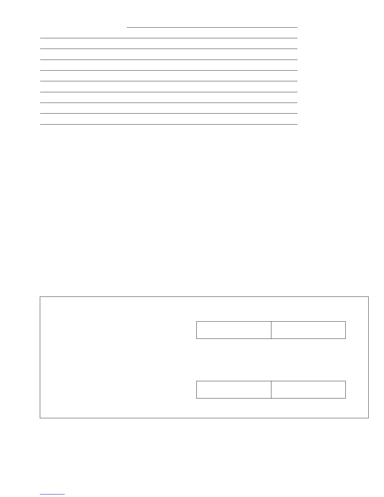
15 8 7 0
Write to TCNT H'FFEC H'5A Write data
15 8 7 0
Write to TCSR H'FFEC H'A5 Write data
Figure 13-2 Writing to TCNT and TCSR
239
Downloaded from Elcodis.com electronic components distributor

 Loading...
