Bit 3
BRLE Description
0P1
3 and P12 function as input/output pins. (Initial value)
1P1
3 functions as the input pin. P12 functions as the output pin.
Bits 2 to 0—Reserved: These bits cannot be modified and are always read as “1.”
9.2.3 Pin Functions in Each Mode
Port 1 operates differently in the expanded modes (modes 1, 2, 3, and 4) and the single-chip mode
(mode 7). Table 9-3 explains how the pin functions are selected in the expanded mode. Table 9-4
explains how the pin functions are selected in the single-chip mode.
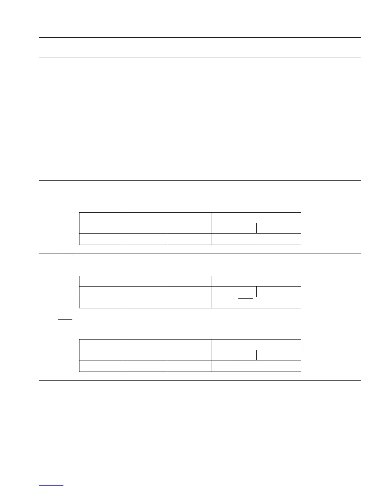
Table 9-3 Port 1 Pin Functions in Expanded Modes
Pin Functions and How they are Selected
P1
7 / TMO The function depends on output select bits 3 to 0 (OS3 to OS0) of the 8-bit timer
control/status register (TCSR) and on the P1
7DDR bit as follows:
OS3 to OS0 All four bits are “0” At least one bit is “1”
P1
7DDR0101
Pin function P1
7 input P17 output TMO output
P1
6 / IRQ1 The function depends on the IRQ1E bit and the P16DDR bit as follows:
IRQ
1E0 1
P1
6DDR0101
Pin function P1
6 input P16 output IRQ1 input
P1
5 / IRQ0 The function depends on the IRQ0E bit and the P15DDR bit as follows:
IRQ
0E0 1
P1
5DDR0101
Pin function P1
5 input P15 output IRQ0 input
145
Downloaded from Elcodis.com electronic components distributor

 Loading...