Table 15-4 A/D Conversion Time (Single Mode)
CKS = “0” CKS = “1”
Item Symbol Min Typ Max Min Typ Max
Synchronization delay t
D 18 — 33 10 — 17
Input sampling time t
SPL —63——31—
Total A/D conversion time t
CONV 259 — 274 131 — 138
Note: Values in the table are numbers of states.
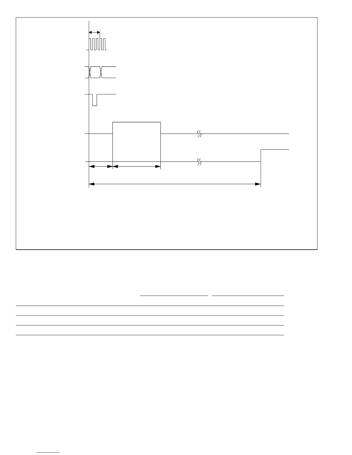
Internal address
bus
Write signal
Input sampling
timing
ADF
ø
(1)
(2)
t
D tSPL
tCONV
(1)
(2)
t
t
t
: ADCSR write cycle
: ADCSR address
: Synchronization delay
: Input sampling time
: Total A/D conversion time
D
SPL
CONV
Figure 15-5 A/D Conversion Timing
288
Downloaded from Elcodis.com electronic components distributor

 Loading...
