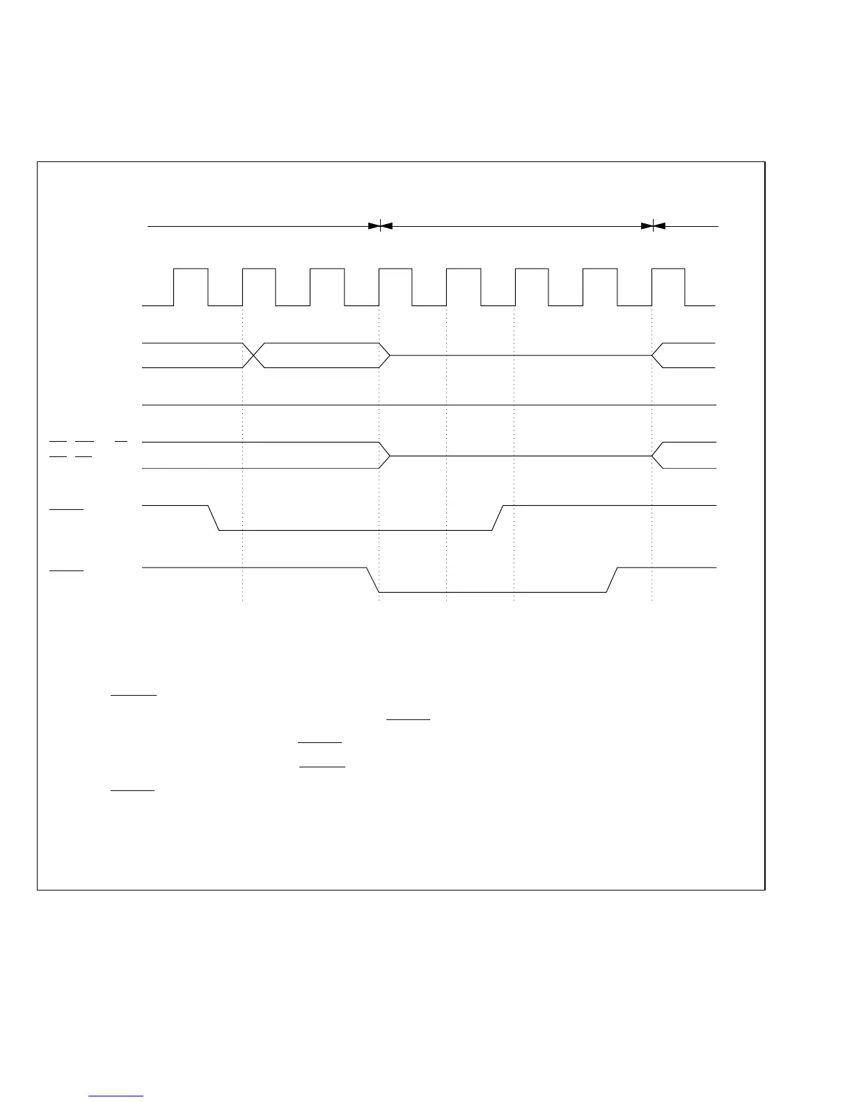
Timing Charts: Timing charts of the operation by which the bus is released are shown in
figure 3-13 for the case of bus release during an on-chip memory read cycle, in figure 3-14 for
bus release during an external memory read cycle, and in figure 3-15 for bus release while the
CPU is performing an internal operation.
RD, WR, R/W
DS, AS
D –D70
A –A19 0
ø
BREQ
BACK
On-chip memory
Access cycle
Bus-right release cycle CPU cycle
T
2 T1 T2 TX TX TX TX T1***
(1) (2) (3) (4) (5)
Fig. 3-13
(1) The BREQ pin is sampled at the start of the T1 state and the Low level is detected.
(2) At the end of the memory access cycle, the BACK pin goes Low and the CPU releases the bus.
(3) While the bus is released, the BREQ pin is sampled at each Tx state.
(4) A High level is detected at the BREQ pin.
(5) The BACK pin is returned to the High level, ending the bus-right release cycle.
* T
1 and T2: On-chip memory access states.
Tx : Bus-right released state.
Figure 3-13 Bus-Right Release Cycle (During On-Chip Memory Access Cycle)
73
Downloaded from Elcodis.com electronic components distributor

 Loading...
