5.4.3 Timing of Interrupt Exception-Handling Sequence
Figure 5-4 shows the timing of the exception-handling sequence for an interrupt when the
program area and stack area are both in on-chip memory and the user-coded interrupt handling
routine starts at an even address.
5.5 Interrupts During Operation of the Data Transfer Controller
If an interrupt is requested during a DTC data transfer cycle, the interrupt is not accepted until the
data transfer cycle has been completed and the next instruction has been executed. This is true
even if the interrupt is an NMI. An example is shown below.
SP
Address
SP
2m – 4
2m – 3
2m – 2
2m – 1
2m
Address
2m – 4
2m – 3
2m – 2
2m – 1
2m
Upper 8 bits of SR
CP
Upper 8 bits of PC
Lower 8 bits of PC
(After)(Before)
Stack area
Save to stack
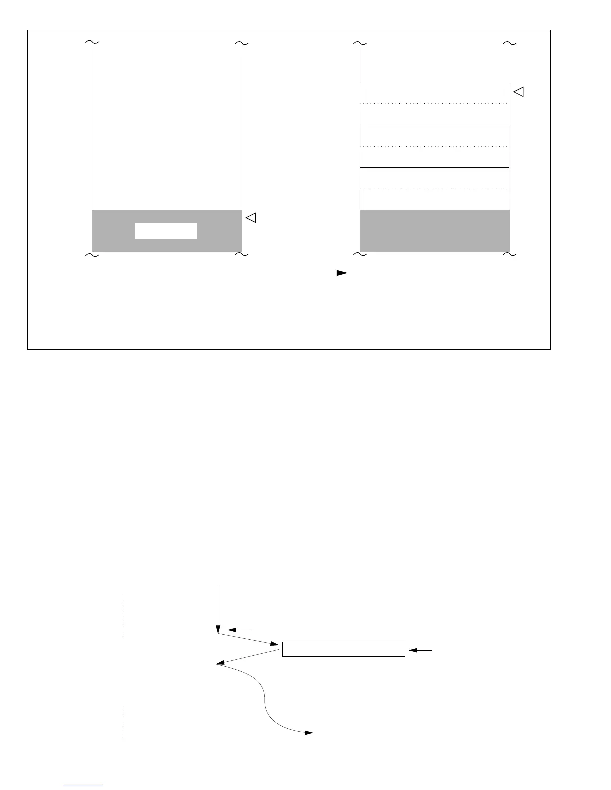
Notes:
1. PC: The address of the next instruction to be executed is saved.
2. Register saving and restoring must start at an even address (e.g 2m).
2m – 5
2m – 6
2m – 5
2m – 6
Lower 8 bits of SR
Don’t care
ADD.W R2, R0
MOV.W R0, @H'FF00
ADD.W @H' FF02,R0
Program flow
DTC interrupt request
Data transfer cycle request NMI interrupt
After data transfer cycle, CPU executes next
instruction before starting exception handling
To NMI exception handling sequence
(Example)
Figure 5-3 (b) Stack before and after Interrupt Exception-Handling
(Maximum Mode)
108
Downloaded from Elcodis.com electronic components distributor

 Loading...
