Appendix C I/O Port Schematic Diagrams
C.1 Schematic Diagram of Port 1
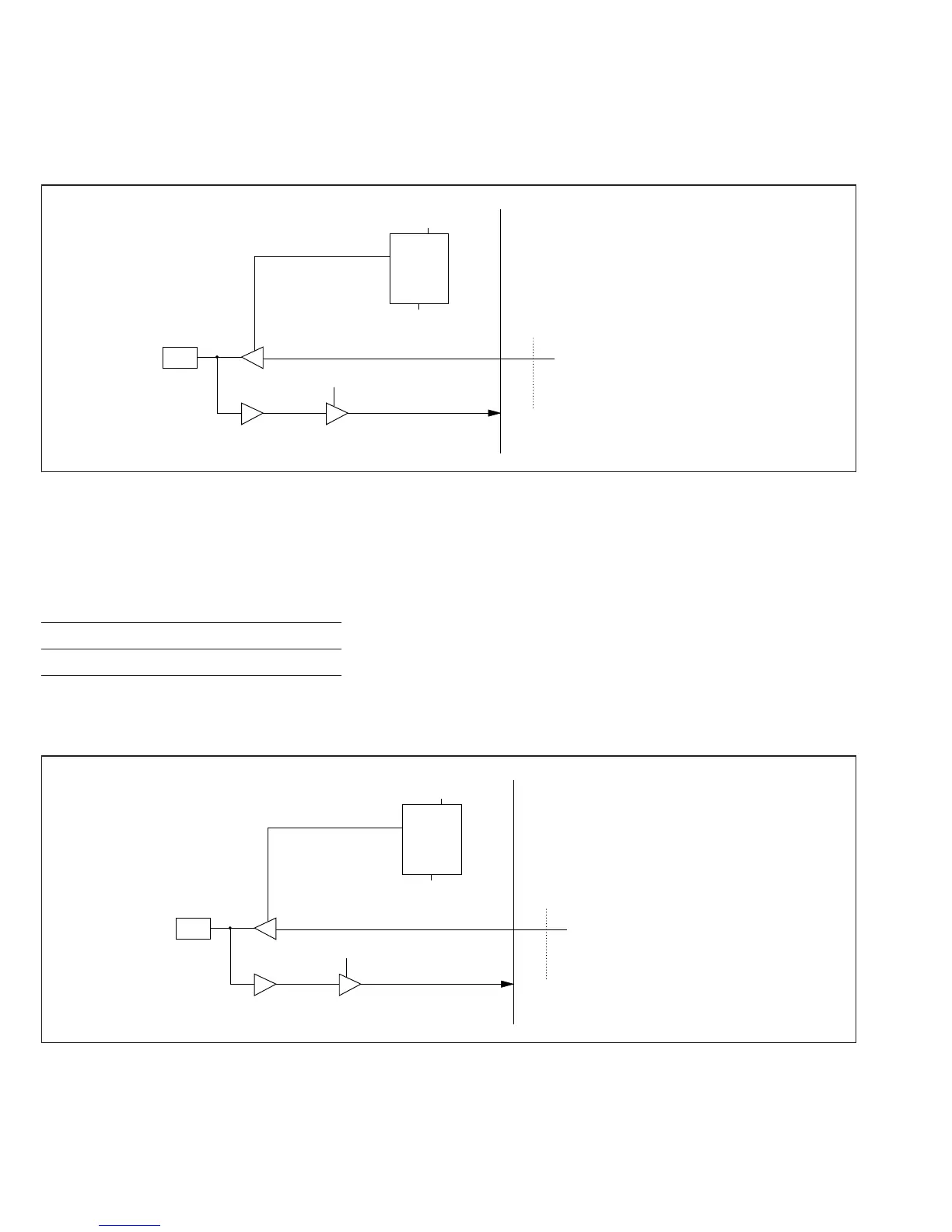
Figure C-1 (a) to (g) gives a schematic view of the port 1 input/output circuits.
Table C-1 (a) Port 1 Port Read (Pin P10)
Setting Port Read Data
DDR = 0 Pin value
DDR = 1 ø
C
R
QD
P1 DDR
0
WP1D
Reset
WP1D:
RP1:
Write to P1DDR
Read Port 1
Internal data bus (PDB8)
P10
ø
RP1
C
R
QD
P1 DDR
1
WP1D
Reset
WP1D:
RP1:
Write to P1DDR
Read Port 1
Internal data bus (PDB9)
P11
E
RP1
Figure C-1 (a) Schematic Diagram of Port 1, Pin P10
Figure C-1 (b) Schematic Diagram of Port 1, Pin P11
407
Downloaded from Elcodis.com electronic components distributor

 Loading...
