20.2.2 AC Characteristics
The AC characteristics of the H8/532 chip are listed in three tables. Bus timing parameters are
given in table 20-4, control signal timing parameters in table 20-5, and timing parameters of the
on-chip supporting modules in table 20-6.
Table 20-4 Bus Timing
Conditions: VCC = 5.0V ±10%, AVCC = 5.0V ±10%, ø = 0.5 to 10MHz, VSS = 0V
Ta = –20 to +75˚C (Regular Specifications)
Ta = –40 to +85˚C (Wide-Range Specifications)
6MHz 8MHz 10MHz Measurement
Item Symbol Min Max Min Max Min Max Unit Conditions
Clock cycle time t
cyc 166.7 2000 125 2000 100 2000 ns See figure 20-4
Clock pulse width Low t
CL 65 – 45 – 35 – ns
Clock pulse width High t
CH 65 – 45 – 35 – ns
Clock rise time t
Cr –15–15–15ns
Clock fall time t
Cf –15–15–15ns
Address delay time t
AD –70–65–65ns
Address hold time t
AH 30 – 25 – 20 – ns
Data strobe delay time 1 t
DSD1 –70–60–40ns
Data strobe delay time 2 t
DSD2 –70–60–50ns
Data strobe delay time 3 t
DSD3 –70–60–50ns
Write data strobe pulse width t
DSWW 200 – 150 – 120 – ns
Address setup time 1 t
AS1 25 – 20 – 15 – ns
- - - - - - - - - - - - -
- - - - - - - - - - - - -
- - - - - - - - - -
- - - - - - - - - -
H8/532
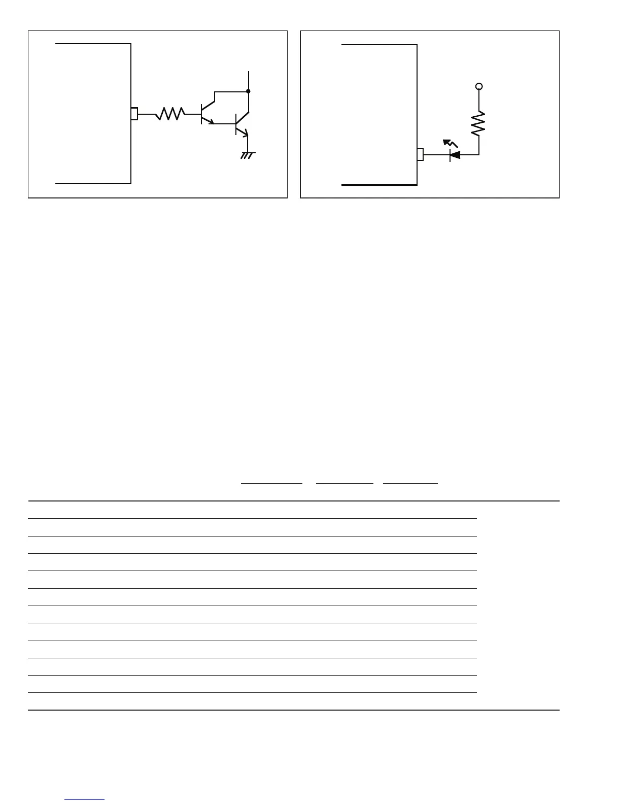
Port
2 kΩ
Darlington pair
Figure 20-1 Example of Circuit for Driving a
Darlington Transistor Pair
Figure 20-2 Example of Circuit for Driving
an LED
322
Downloaded from Elcodis.com electronic components distributor

 Loading...
