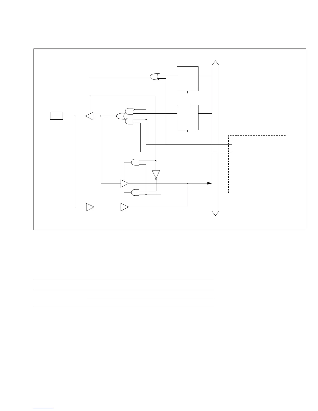
C.9 Schematic Diagram of Port 9
Figure C-9 (a) to (e) gives a schematic view of the port 9 input/output circuits.
Table C-9 (a) Port 9 Port Read (Pins P90, P91)
Setting Port Read Data
Output enable Output compare output value
DDR = 0 Pin value
DDR = 1 DR value
RP9
P9
n
WP9
Free-running timer module
Output enable
Output compare output
WP9D:
WP9:
RP9:
n:
Write to P9DDR
Write to Port 9
Read Port 9
0 or 1
Internal data bus (PDB8, PDB9)
C
R
QD
P9 DR
n
C
R
QD
P9 DDR
n
Reset
Reset
WP9D
Output disable
Figure C-9 (a) Schematic Diagram of Port 9, Pins P90 and P91
424
Downloaded from Elcodis.com electronic components distributor

 Loading...
