2000-OSM, F1 8-59
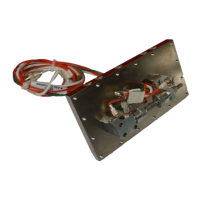
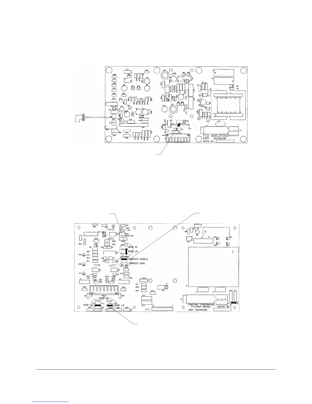
FID Amplifier PCB
The jumper on this PCB relates to intercolumn detector usage. For normal operation shunts should
be installed in the first two positions at the right side of J18. These shunts are removed for an
application using intercolumn detectors (see Figure 8-32).
J18
Figure 8-32. FID AMPLIFIER PCB JUMPER LOCATIONS
Filament TCD Amplifier PCB
The jumpers on this PCB relate to amplifier gain, single or dual carrier, temperature ranges,
intercolumn detectors, and special testing (see Figure 8-33 for location).
GAIN JUMPERS
WT11 - WT13
CARRIER JUMPERS
WT7 - WT10
TEMPERATURE JUMPERS
WT1 - WT6
Figure 8-33. FILAMENT TCD AMPLIFIER PCB JUMPER LOCATIONS
The gain jumper is normally connected between WT11 and WT12. For high gain applications this
jumper is connected between WT12 and WT13.
 Loading...