Video Input
Jetson AGX Xavier Series Product DG-09840-001_v2.5 | 93
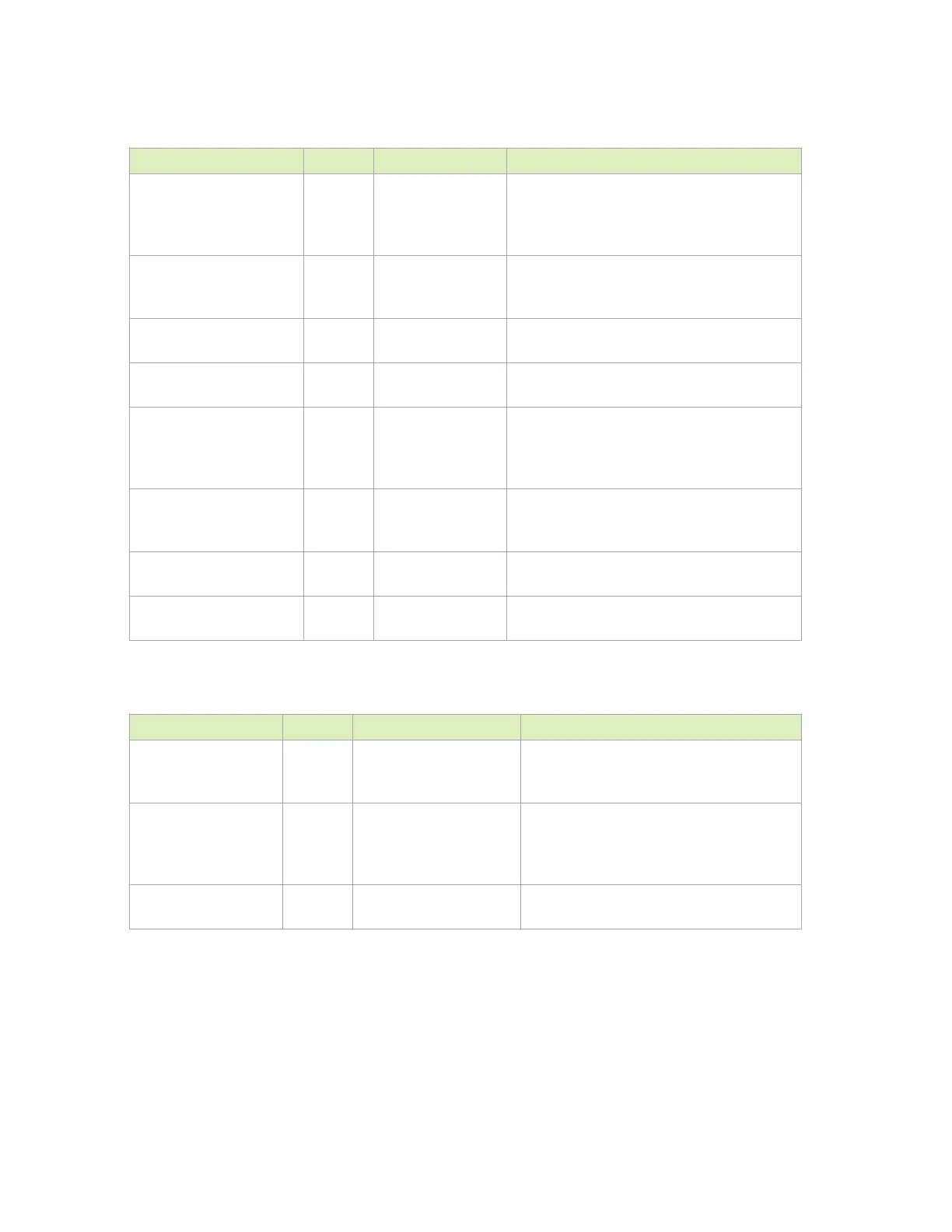
Table 10-13. SLVS Camera Signal Connections
Module Pin Name Type Termination Description
NVHS0_SLVS_RX[7:0]_N/P DIFF IN
SLVS Differential Data Lanes: Connect lanes [7:0]
to matching [7:0] pins on SLVS device/connector.
Reverse connections ([7:0] to SLVS
NVHS0_SLVS_REFCLK_N/P DIFF IN
SLVS Differential Reference Clock: Connect to
second output (DIF1 in figure) of a suitable clock
buffer.
GPIO18 (XHS) O
Horizontal Sync: Connect to matching pins of SLVS
GPIO19 (XVS) O
Vertical Sync: Connect to matching pins of SLVS
device/connector
SPI2_CLK
SPI2_MOSI
SPI2_MISO
O
O
I
SPI #2 Clock, Master Out / Slave In and Master In /
Slave Out: Connect to matching pins on SLVS
device/connector (CLK to CLK, MOSI to MOSI and
I2C3_CLK
I2C3_DAT
I/OD
I/OD
I2C #3: Optional alternative control interface.
Connect to matching pins of SLVS
device/connector instead of SPI.
SPI3_MOSI (XCE) O
Chip Enable: Connect to matching pins of SLVS
SPI3_MISO (XCLR) O
Clear: Connect to matching pins of SLVS
device/connector
Table 10-14. Non-Module SLVS Reference Clock Connections
Function Type Termination Description
OSC_OUTN/P DIFF OUT
33Ω series resistors and
49.9Ω, 1% pulldowns to
Reference Clock Differential Oscillator Outputs:
Connect differential oscillator output to
matching pins on differential clock buffer pins.
CLOCK_BUFFER_DIF0 DIFF OUT
150Ω, 1% pulldowns to
GND on each line. 100Ω
resistor between the P/N
lines.
Differential Clock Buffer Output #1: Connect to
LVDS-CMOS device inputs.
LVDS-CMOS Output O
LVDS-CMOS converter output: Connect to SLVS
device/connector input clock (INCK in figure)

 Loading...


