Debug and Strapping
Jetson AGX Xavier Series Product DG-09840-001_v2.5 | 119
Module Pin
Name (other)
Type Termination Description
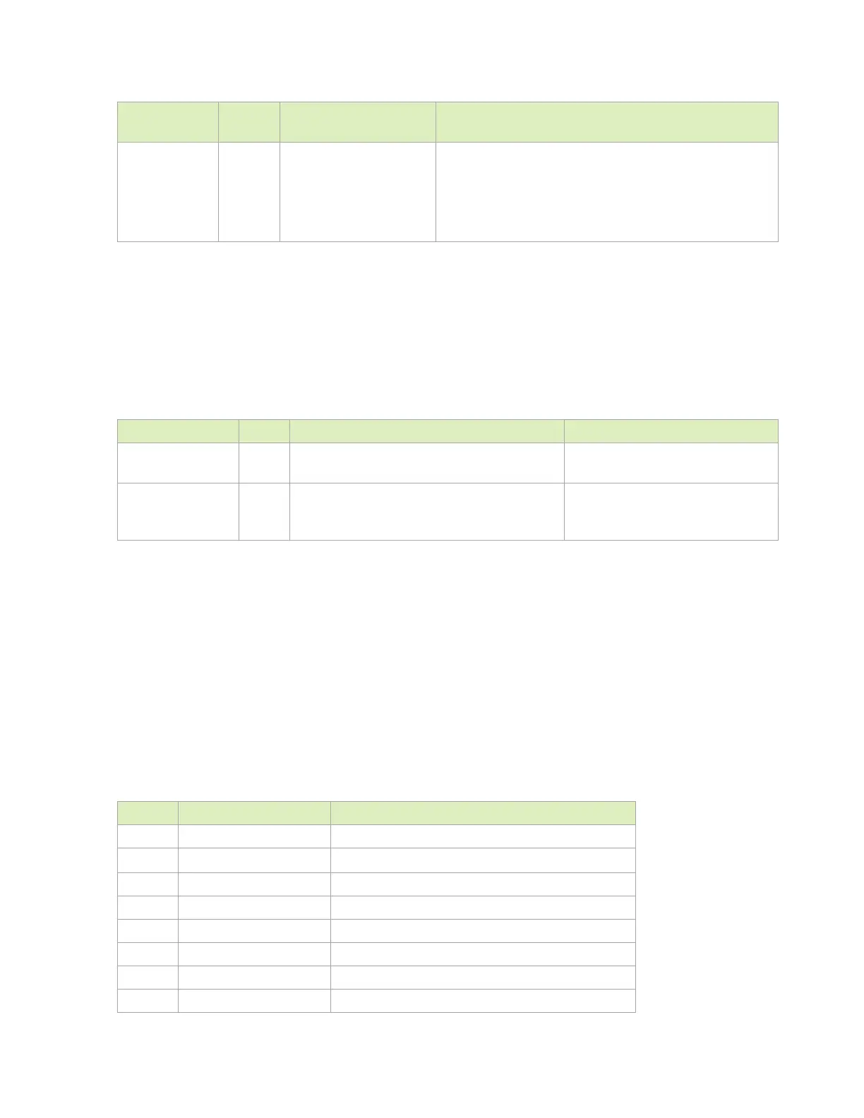
NVDBG_SEL 100kΩ to GND on module NVIDIA Debug Select: Used as select
Normal operation: Leave series resistor from NVDBG_SEL not
stuffed.
Advanced Debug modes: Connect NVDBG_SEL to VDD_1V8
(install 0Ω resistor as shown).
15.2.2 Debug UART
Jetson AGX Xavier provides UART3_DEBUG for debug purposes. The connections are
described in the following table.
Table 15-3. Debug UART Connections
Module Pin Name Type Termination Description
UART3_TX_DEBUG O UART Transmit: Connect to RX pin
of serial device
UART3_RX_DEBU
G
I If level shifter implemented, 100kΩ to supply
on the non-Jetson AGX Xavier side of the
device.
UART Receive: Connect to TX pin
of serial device
15.3 Strapping Pins
Jetson AGX Xavier has one strap (FORCE_RECOVERY_N) that is intended to be used on the carrier
board. That strap is used to enter Force Recovery mode (held low during power-on). The other
straps mentioned in this section are for use on the module by NVIDIA only. Their state at
power-on must not be affected by any connections on the carrier board. The carrier board
design should guarantee a high-z on the pins during boot. The pins that are associated with
SoC straps (besides
FORCE_RECOVERY_N) are as follows:
Table 15-4. Strapping Pins
Pin # Pin Name Description
L10 FORCE_RECOVERY_N USB Recovery Strap
E10 GPIO12
Boot Chain Select (JAXi only – See Table 15-4)
L11 STANDBY_REQ_N On-Module use only
L4 UART4_RTS “
L5 UART4_TX “
K53 UART1_TX “
K58 UART1_RTS “
K58 UART5_RTS “

 Loading...


