Audio
Jetson AGX Xavier Series Product DG-09840-001_v2.5 | 101
12.1.1 I2S Design Guidelines
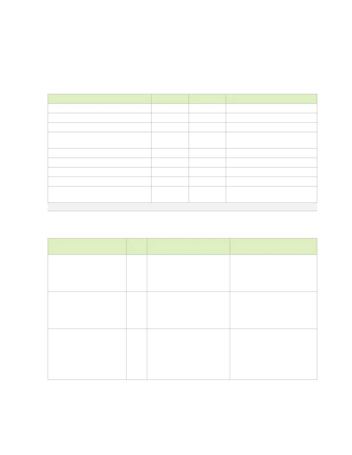
The following table details the signal routing requirements for the I2S interface.
Table 12-3. I2S Interface Signal Routing Requirements
Parameter Requirement Units Notes
Configuration / Device Organization 1 load
Max Loading 8 pF
Reference plane GND
Breakout Region Impedance
Min
width/spacing
Trace Impedance 50 Ω ±20%
Via proximity (Signal to reference) < 3.8 (24) mm (ps) See Note 1
Trace spacing - Microstrip or Stripline 2x dielectric
Max Trace Delay 540 (3400) mm (ps)
Max Trace Delay Skew between SCLK and
SDATA_OUT/IN
38 (240) mm (ps)
Note: Up to 4 signal Vias can share a single GND return Via
Table 12-4. I2S and Miscellaneous Codec Signal Connections
Module Pin Name (Xavier
Function)
Type Termination Description
I2S1_SCLK (I2S1_CLK)
I2S2_SCLK (I2S2_CLK)
I2S3_SCLK (I2S4_CLK)
JAX: GPIO21 (I2S6_CLK)
JAXi: No I2S support. GPIO only.
I/O
120Ω Bead in series and 2.7pF
capacitor to GND (on Jetson AGX
Xavier).
I2S Serial Clock: Connect to I2S/PCM
CLK pin of audio device.
I2S1_FS (I2S1_LRCK)
I2S2_FS (I2S2_LRCK)
I2S3_FS (I2S4_LRCK)
JAX: GPIO20 (I2S6_LRCK)
JAXi: No I2S support. GPIO only.
I/O
I2S Left/Right Clock: Connect to
Left/Right Clock pin of audio device.
I2S1_DOUT (I2S1_SDOUT)
I2S2_DOUT (I2S2_SDOUT)
I2S3_DOUT (I2S4_SDOUT)
JAX: GPIO05 (I2S6_SDOUT)
JAXi: No I2S support. GPIO05
connected to CAN0_ERR on
module.
I/O
I2S Data Output: Connect to Data Input
pin of audio device.

 Loading...


