Miscellaneous Interfaces
Jetson AGX Xavier Series Product DG-09840-001_v2.5 | 109
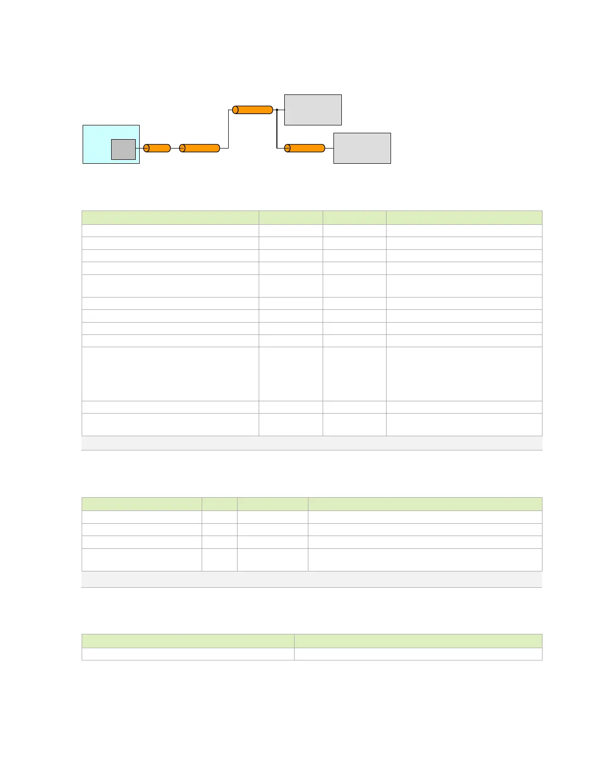
Figure 13-6. SPI Daisy Topologies
Module
SPI
Device #1
Main trunk
SPI
Device #2
Die
PK G
Branch
-A
Branch-B
Table 13-7. SPI Interface Signal Routing Requirements
Max Frequency 65 MHz
Configuration / Device Organization 3 load
Max Loading (total of all loads) 15 pF
Reference plane GND
Breakout Region Impedance
Minimum width
& spacing
Max PCB breakout delay 75 ps
Trace Impedance 50 – 60 Ω ±15%
Via proximity (Signal to reference) < 3.8 (24) mm (ps) See Note
Trace spacing - Microstrip / Stripline 4x / 3x dielectric
Max Trace Length/Delay (total)
For
and
134 (787)
109 (685)
129 (815)
mm (ps)
Max Branch delay 75ps
Max Trace Length/Delay Skew from
and
to
16 (100) mm (ps) At any point
Note: Up to 4 signal vias can share a single GND return via.
Table 13-8. SPI Signal Connections
Module Pin Names Type Termination Description
I/O
SPI Clock.: Connect to Peripheral CLK pin(s)
I/O
SPI Data Output: Connect to Slave Peripheral MOSI pin(s)
I/O
SPI Data Input: Connect to Slave Peripheral MISO pin(s)
SPI[3:1]_CS[1:0]_N,
SPI2_CS0_N
I/O
SPI Chip Selects.: Connect one CS_N pin per SPI IF to each
Slave Peripheral CS pin
Note: JAXi only: SPI2 routed to safety MCU if implemented in design
Table 13-9. Recommended SPI Observation Test Points for Initial Boards
Test Points Recommended Location
One for each SPI signal line used
Near Jetson AGX Xavier and Device pins.

 Loading...


