SDIO and SD Card
Jetson AGX Xavier Series Product DG-09840-001_v2.5 | 95
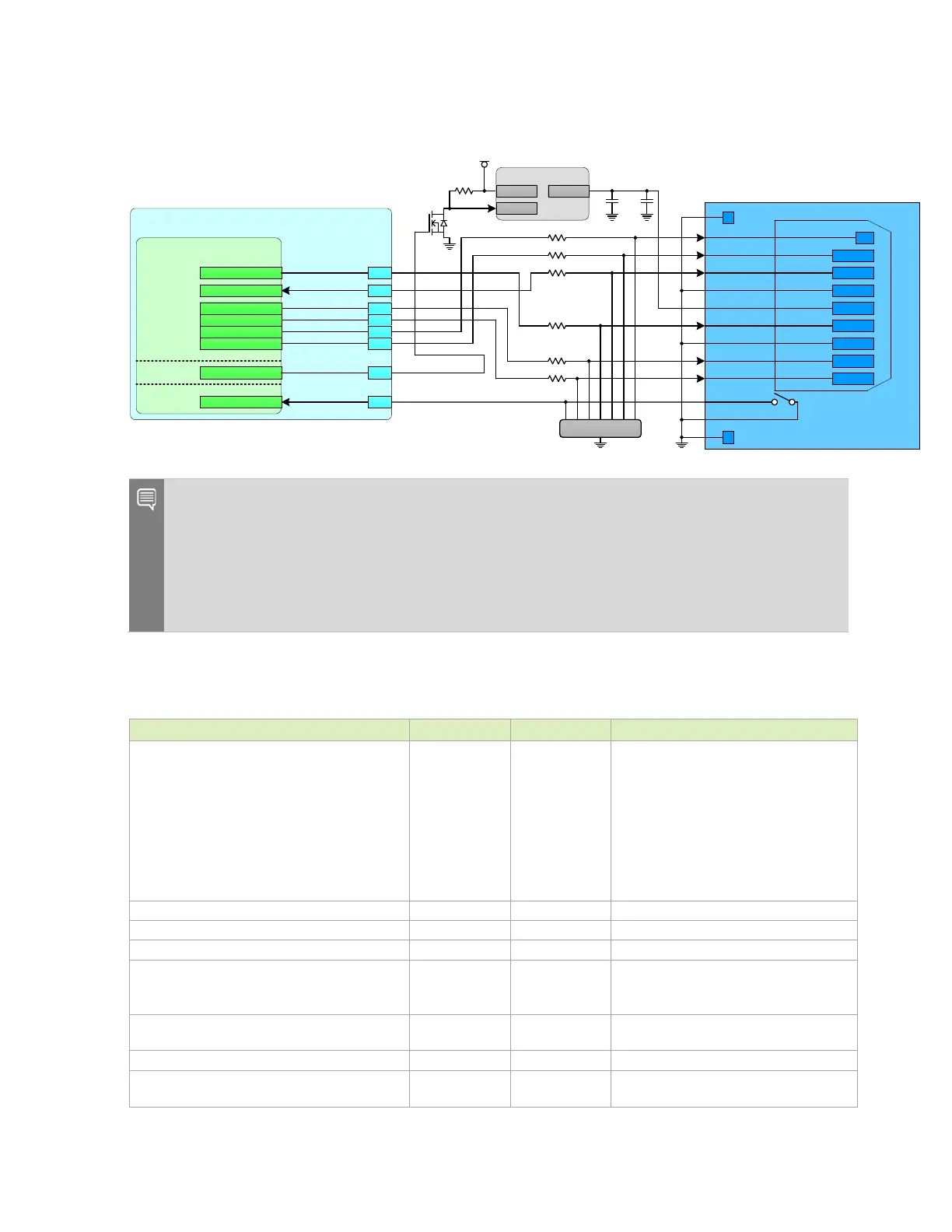
Figure 11-1. Micro SD Card Socket Connection Example
ESD
DATA2
DATA3
CMD
VDD
CLK
GND
DATA0
DATA1
C_DETECT
COMMON
VDD_3V3
Load S witch
VO UTVIN
ON
SDMMC_V DD_E N
GND
10Ω
10
Ω
10Ω
0Ω
10Ω
10Ω
4. 7k
Ω
G
S
D
Jetson AGX Xavier
SDMMC1_ CD*
SoC
SDMMC1
SDMMC1_CLK
SDMMC1_CMD
CONN
SDMMC1_DAT3
SOC_GPIO11
UART1_RX
SDCARD_CLK
SDCARD_CMD
SDCARD_D0
SDCARD_D1
SDCARD_D2
SDCARD_D3
GP IO 21
GP IO 02
SDMMC1_DAT2
SDMMC1_DAT1
SDMMC1_DAT0
A5
B6
L6
B5 8
E8
F8
A4
D6
CAM
Notes:
1. If EMI and/or ESD devices are necessary, they must be tuned to minimize the impact to signal
quality, which must meet the timing and Vil/Vih requirements at the receiver and maintain
signal quality and meet requirements for the frequencies supported by the design.
2. Supply (load switch, etc) used to provide power to the SD Card must be current limited if the
supply is shorted to GND.
Table 11-3. SDCARD Interface Signal Routing Requirements
Parameter Requirement Units Notes
Max Frequency 3.3V Signaling
DS
HS
Max Frequency 1.8V Signaling
SDR12
SDR25
SDR50
SDR104
DDR50
25 (12.5)
50 (25)
25 (12.5)
50 (25)
100 (50)
208 (104)
50 (50)
MHz (MB/s)
See Note 1
Topology Point to point
Reference plane
or
See Note 2
Trace Impedance 50 Ω ±15%. 45Ω optional depending on stack-up
Max Via Count
PTH
HDI
Independand of stackup layers
Depends on stackup layers
Via proximity (Signal to reference)
< 3.8 (24) mm (ps)
Up to 4 signal Vias can share 1
return
Via
Trace spacing – Microstrip / Stripline 4x / 3x dielectric
Trace length
SDR50 / SDR25 / SDR12 / HS / DS

 Loading...


