Jetson AGX Xavier Series Product DG-09840-001_v2.5 | 77
Chapter 10. Video Input
Jetson AGX Xavier provides multiple MIPI CSI D-PHY or C-PHY interfaces for cameras. In
addition, an 8-lane SLVS camera interface is supported.
10.1 MIPI CSI
Jetson AGX Xavier supports four MIPI CSI x4 bricks, allowing a variety of device types and
combinations to be supported. Up to 4 quad lane cameras or four dual lane cameras plus two
quad lane cameras or 6 dual lane cameras (total of 6 in any configuration) are available. Both
MIPI D-PHY and C-PHY modes are supported. In D-PHY mode, each data channel has peak
bandwidth of up to 2.5Gbps. For C-PHY, each lane (Trio) supports up to 1.7 Gsps.
Note: Maximum data rate may be limited by use case and memory bandwidth.
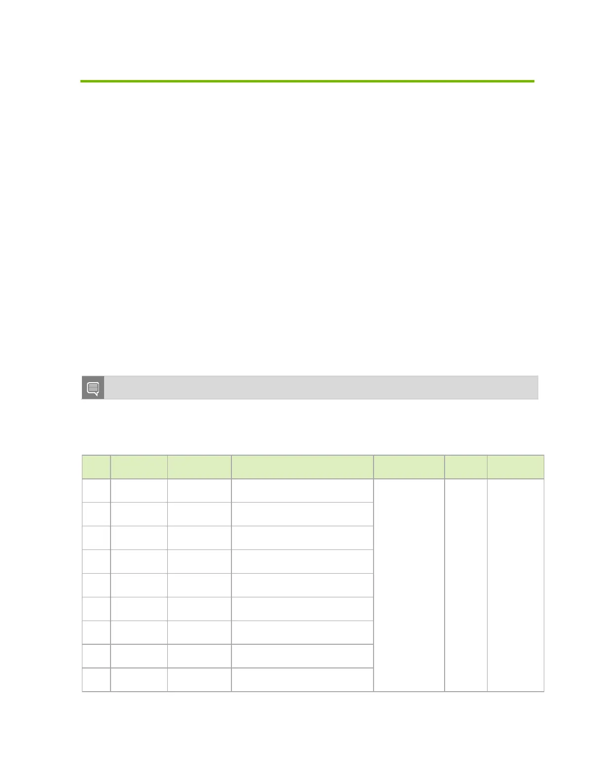
Table 10-1. Jetson AGX Xavier CSI Pin Description
Pin #
Module Pin
Name
SoC Signal Usage/Description
Usage on NVIDIA
Carrier Board
Direction Pin Type
F42 CSI0_CLK_N CSI_A_CLK_N
Camera, CSI 0: DPHY Clock–, CPHY
01:C
Camera Connector Input
MIPI D-PHY/C-
PHY
F43 CSI0_CLK_P CSI_A_CLK_P
Camera, CSI 0: DPHY Clock+. CPHY
00:C
E41 CSI0_D0_N CSI_A_D0_N
Camera, CSI 0: DPHY Data 0–. CPHY
00:B
E42 CSI0_D0_P CSI_A_D0_P
Camera, CSI 0: DPHY Data 0+. CPHY
00:A
E38 CSI0_D1_N CSI_A_D1_N
Camera, CSI 0: DPHY Data 1–. CPHY
01:B
E39 CSI0_D1_P CSI_A_D1_P
Camera, CSI 0: DPHY Data 1+. CPHY
01:A
H42 CSI1_CLK_N CSI_B_CLK_N
Camera, CSI 1: DPHY Clock–, CPHY
11:C
H43 CSI1_CLK_P CSI_B_CLK_P
Camera, CSI 1: DPHY Clock+. CPHY
10:C
G42 CSI1_D0_N CSI_B_D0_N
Camera, CSI 1: DPHY Data 0–. CPHY
10:B

 Loading...


