USB, PCIe, and UFS
Jetson AGX Xavier Series Product DG-09840-001_v2.5 | 54
Within pair (intra-pair) matching between
subsequent discontinuities
Differential pair uncoupled length
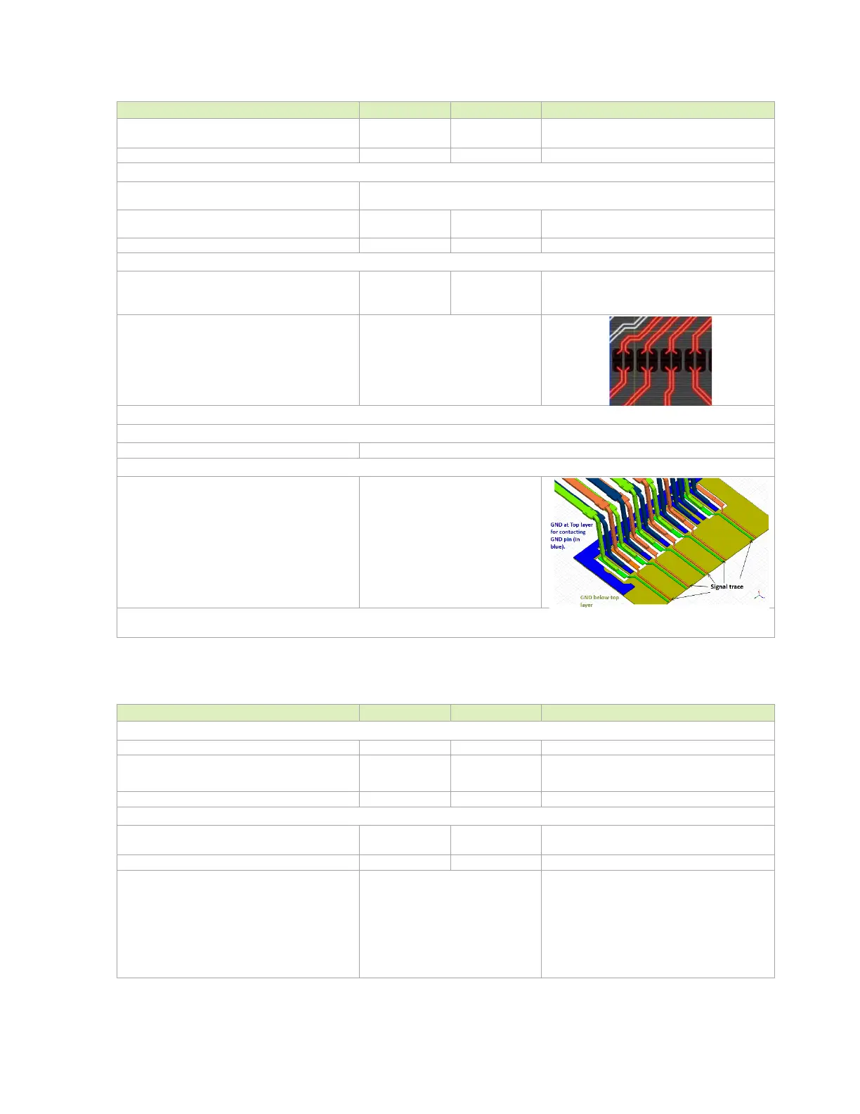
Place GND vias as symmetrically as possible to data pair vias. GND via distance should
be placed less than 1x the diff pair via pitch
Use micro via or back drilled via - no via stub
allowed.
20%, 0402 X5R or better. Only required
for TX pair when routed to connector.
Place close to TX side.
Voiding the plane directly under
the pad 3-4 mils larger than the
pad size is required.
Serpentine (See USB 3.1 Guidelines)
Remove unwanted GND fill that is either floating or act like antenna
Void all layers of golden finger
area under the pad 5.7 mils
larger than the pad size is
recommended.
Keep critical PCIe traces such as PEX_TX/RX, TERMP etc. away from other signal traces or unrelated power traces/areas or
power supply components
Table 7-14. PCIe Signal Connections Module I/Fs Configured as Root Ports
8.0GHz, half-rate architecture
Unidirectional,
differential. Driven by
100MHz common reference clock
To GND Single Ended for P and N
Trace Impedance
differential / Single Ended
• Use spread-glass
(denser weave) instead
of regular-glass
(sparse weave) to
minimize intra-pair
skew
Example of zig-zag routing

 Loading...


