Power
Jetson AGX Xavier Series Product DG-09840-001_v2.5 | 25
Note: OD – Open-drain. PP = Push-pull.
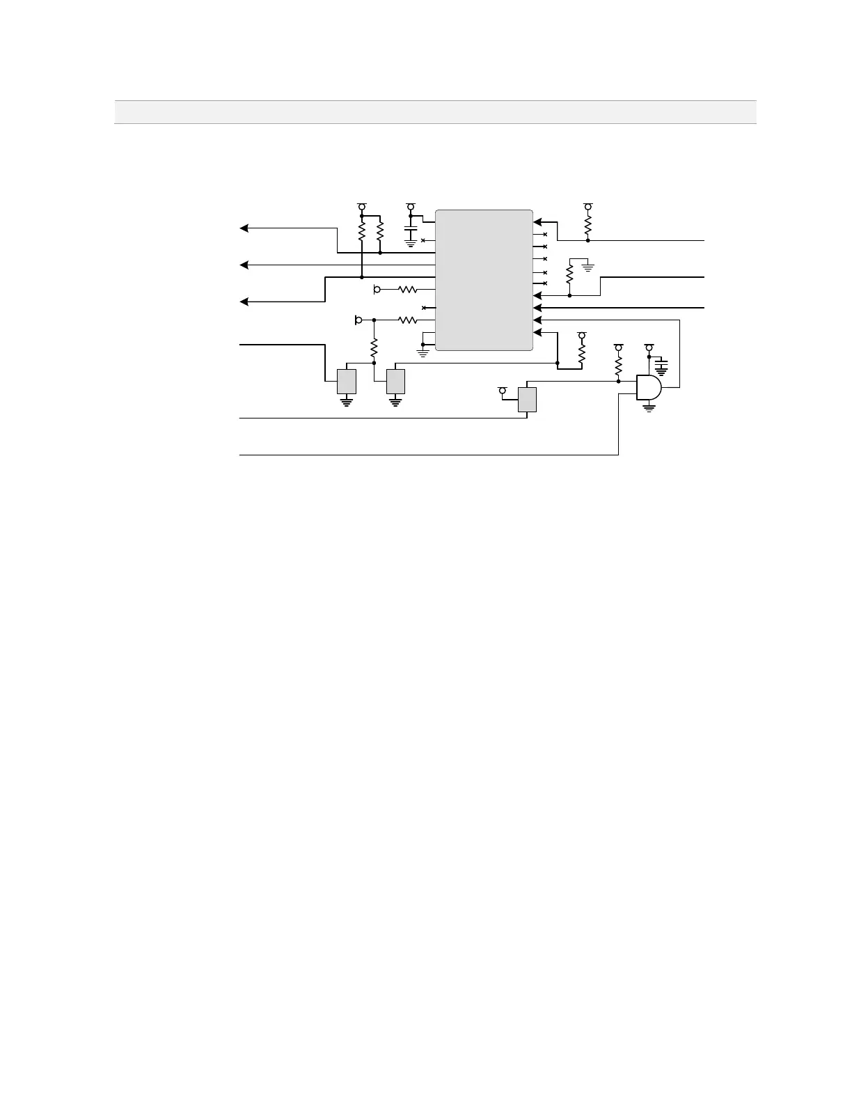
Figure 5-8. Power-On Button Circuit
To Module (Pin L5 4)
POWER_BTN_N
G
D
S
FET
3V 3_ AO
VIN_PWR_ON
VDD_3V3
G
D
S
FET
CARRIER_POWER_ON
3V 3_ AO
G
D
S
FET
From Mod ul e ( Pi n L62 )
From Po we r Button
VDDIN_PWR_BAD_N
VDD_5V
3V3_AO
MODULE_POWER_O N
From VIN Loss Detection
& ot her s ourc es
(Modu le Pi n L55 )
3V3_AO
NT S40 01
NT 1G
0. 1uF
4. 7kΩ
10 kΩ
10 kΩ
EFM8SB10F8G
VDD
P1.7
P1.6
P1.5
P1.3
P1.2
P2.7_C2D
RST*_C2CK
GND
EP AD
P0.0
P0.1
P0.2
P0.3
P0.4
P0.5
P0.6
P0.7
P1.0
P1.1
10 kΩ
3V 3_ AO
10 kΩ
BUTTON_POWER_ON*
ACOK
OVERTEMP_N (FORCE_SHUTDOWN)
SYS_RESET_N
10 kΩ
10 kΩ
5V_AO
From Mod ul e ( Pi n L52 )
10 0k Ω
3V 3_ AO
10 kΩ
VCC_SRC &
VDD_5V enable
To Module (Pin L6 1)
To Module (Pin L6 0)
Used to opt in ally e nable
Au to
-Power-On
5.4.2.1 Defined behaviors
For all actions triggered by BUTTON_POWER_ON*, there will be a de-bounce time before
triggering any output signal. All timings below are referenced from AFTER the de-bouncing.
Therefore, a “0 ms” value indicates that the signal should start right after de-bounce. De-
bounce time is 20 ms.
5.4.2.2 Power OFF -> Power ON (Power Button Case)
Power button press use case: User presses the Power Button briefly, and the MCU sends the
power enable signals to the module (
VIN_PWR_ON) and to the PMIC on the module
(
MODULE_POWER_ON). The signal representing the power button to Jetson AGX Xavier
(
POWER_BTN_N), will have the same (brief) duration of the Power Button input to the MCU. Once
the power button is pressed, the power OK input (ACOK) is ignored, as the power ON sequence
is already initiated by the power button.

 Loading...


