Power
Jetson AGX Xavier Series Product DG-09840-001_v2.5 | 24
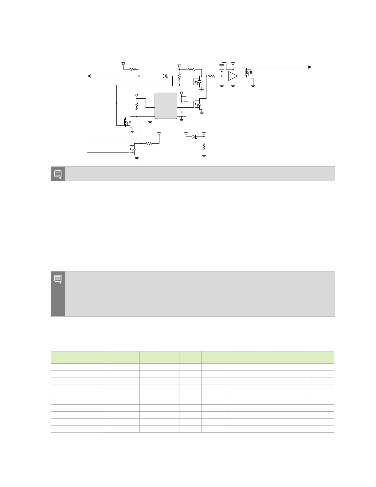
Figure 5-7. Optional ACOK Circuitry
G
S
D
5V _AO_ON KEY
0.1uF
24 0Ω, 1%
0.47uF
4. 75 kΩ, 1%
10 kΩ, 1%
G
S
D
G
S
D
5V _AO_ON KEY
0.1uF
4. 75 k
Ω, 1%
VDD_1V8
ACOK_AP_L
ACOK_L
SN74LVC1G74
DQER-DFN08
VCCSD*
QD
CP Q*
RD GND
5V _AO_ON KEY
G
S
D
5V_AO _PGD
G
S
D
5V _AO_ON KEY
CARRIER_PWR_ON
47.5kΩ, 1%
5V _AO_ON KEY
Pull ed lo w fo r
Au to-Power-On
or conne cted
to charger
ACOK output
From Modul e
(Pin L62)
4. 75 kΩ, 1%
5V_AO 5V _AO_ON KEY
From Powergood
on 5V_AO Supp ly
To Module
VCOMP_ALERT_N
(Pin F61)
10 0kΩ, 1%
Optional ACOK circuit Output
See note
Note: See Figure 5-6.
5.4.2 Power Button Supervisor MCU Power-On
The NVIDIA Jetson AGX Xavier carrier board implements a power button supervisor. This
supervisor is a low power device meant to intercept push-button (momentary) switches to
control ON/Enable signals to the module PMIC and main processor. This supervisor is always
powered and allows close to complete system power OFF while providing proper timing for
ON/OFF signals to the system. The selected MCU to perform this function is the
EFM8SB10F8G-A-QFN20 from Silicon Labs.
Note: Designs that intend to follow the NVIDIA carrier board design and include the
EFM8SB10F8G-A-QFN20 MPU for Button Power Button control need to replicate the circuitry on
the latest P2822 carrier board exactly. NVIDIA will provide the binary and the customer should
get the flashing instructions from Silicon Labs. Otherwise, another solution such as the one
described earlier in the Power-On (No MCU) can be used.
Table 5-4. Power Button Supervisor Control Signals
Signal Name Associated
Module Pin #
I/O Type Trigger
Level
Drive
Mode
Description MCU Pin
BUTTON_POWER_ON* Input (debounced) Level OD (HiZ) Power Button P0.0
ACOK Input (debounced) Edge OD (HiZ) Determine when USB power is supplied P0.6
CARRIER_POWER_ON L62 Input Level OD (HiZ) Closed loop on power output P0.7
RESET_N (SYS_RESET_N) L60 Input Edge OD (HiZ) Monitor / Power Good mask P1.1
FORCE_SHUTDOWN_N
(OVERTEMP_N)
L52 Input Level OD (HiZ) Triggers shutdown sequence P1.0
BRD_SEL Input OD (HiZ) Strap pin for board selection P1.2
VIN_PWR_ON Output PP Enable power to module P1.3
MODULE_POWER_ON L54 Output PP Enable input to PMIC P1.5
POWER_BTN_N L61 Output OD Buffered output of power button signal P1.6

 Loading...


