USB, PCIe, and UFS
Jetson AGX Xavier Series Product DG-09840-001_v2.5 | 53
7.2.2 PCIe Gen4 Design Guidelines
The following table details the PCIe design guidelines for Gen4.
Table 7-13. PCIe Gen4 Interface Signal Routing Requirements
8.0GHz, half-rate architecture
Unidirectional,
differential. Driven by
100MHz common reference clock
To GND Single Ended for P and N
Trace Impedance
differential / Single Ended
• Use spread-glass
(denser weave) instead
of regular-glass
(sparse weave) to
minimize intra-pair
skew
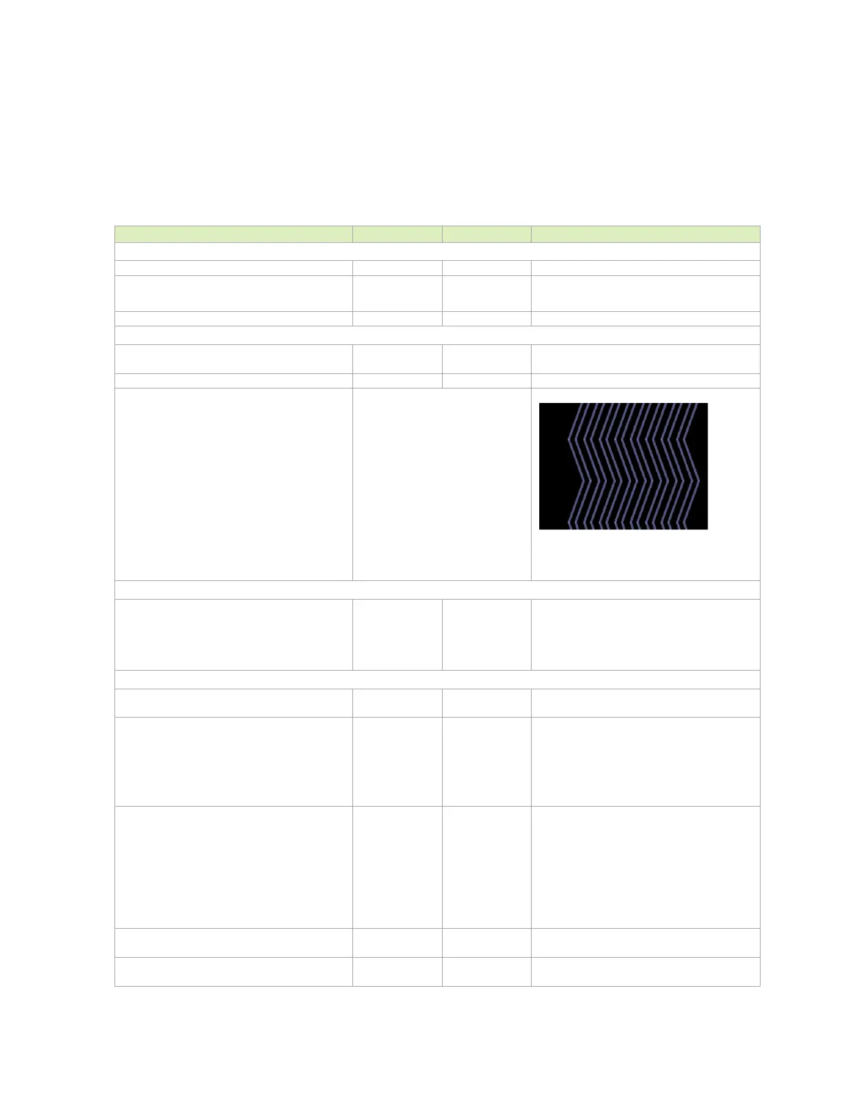
• Use zig-zag route
instead of straight to
minimize skew, this is
a mandatory for PCIe
gen4 design
Example of zig-zag routing
Trace Spacing (Stripline)
Pair – Pair
To plane and capacitor pad
To unrelated high-speed signals
4x
4x
4x
Dielectric
TX and RX should not be routed on the
same layer. If this is required in a design,
they should not be interleaved, and the
spacing between the closest RX and TX
lanes must be 9x Dielectric spacing.
Breakout region (Max Length)
Minimum width and spacing. 4x or wider
dielectric height spacing is preferred
Trace loss budget (for carrier board routing)
Routing direct to device
Routing to PCIe/M.2 connector
-19
-13.5
dB/in
@ 4GHz (See TBD),
Loss: GEN4 budget – module – end device
(-28dB + 5dB + 4dB)
Loss: GEN3 budget – module – end device
(-28dB + 5dB + 9.5dB)
Max trace length (delay)
Direct to device on carrier board
Stripline
Microstrip
Routed to PCIe or M.2 connector
Stripline
Microstrip
357 (2463)
328 (1939)
254 (1750)
233 (1378)
in (ps)
Mid-loss PCB of 1.47dB/in (Microstrip) or
1.35dB/in (Stripline) is used. Also,
6.9ps/mm for Stripline routing and
5.9ps/mm for Microstrip.
Max PCB via distance from the
Device/Connector
Max distance from Device ball or Connector
pin to first PCB via.
PCB within pair (intra-pair) skew
Do trace length matching before hitting
discontinuities.

 Loading...


