General Routing Guidelines
Jetson AGX Xavier Series Product DG-09840-001_v2.5 | 36
Max Trace Lengths/Delays
Trace lengths/delays should include main PCB routing and any additional routing on a
Flex/ secondary PCB segment connected to main PCB. The max length/delay should be
from Jetson AGX Xavier to the actual connector (i.e. USB, HDMI, SD Card, etc.) or device
(i.e. onboard USB device, Display driver IC, camera imager IC, etc.)
Trace Delay/Flight Time Matching
Signal flight time is the time it takes for a signal to propagate from one end (driver) to the
other end (receiver). One way to get same flight time for signal within signal group is to
match trace lengths within specified delay in the signal group.
• Total trace delay = Carrier PCB trace delay only. Do not exceed maximum trace delay
specified.
• For six layers or more, it is recommended to match trace delays based on flight time of
signals. For example, outer-layer signal velocity could be 5.9 ps/mm and inner-layer
6.9 ps/mm If one signal is routed 254 mm on outer layer and second signal is routed
254 mm in inner layer, difference in flight time between two signals will be 300 ps! That
is a big difference if required matching is 15 ps (trace delay matching). To fix this, inner
trace needs to be 43 mm shorter or outer trace needs to be 51 mm longer.
• In this design guide, terms such as intra-pair and inter-pair are used when describing
differential pair delay. Intra-pair refers to matching traces within differential pair (for
example, true to complement trace matching). Inter-pair matching refers to matching
differential pairs average delays to other differential pairs average delays.
6.5 General PCB Routing Guidelines
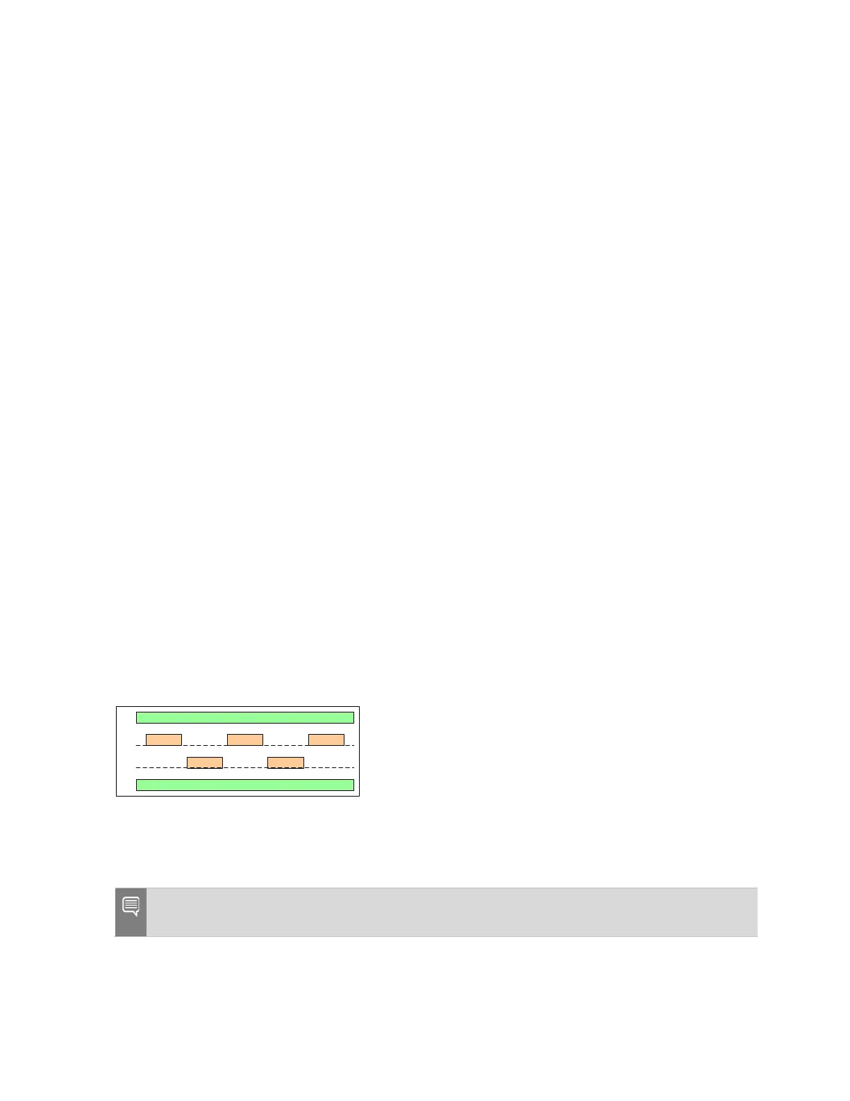
For GSSG stack-up to minimize crosstalk, signal should be routed in such a way that they are
not on top of each other in two routing layers (Figure 6-1).
Figure 6-1. Signal Routing Example
Do not route other signals or power traces and areas directly under or over critical high-speed
interface signals.
Note: The requirements detailed in the interface signal routing requirements tables must be met
for all interfaces implemented or proper operation cannot be guaranteed.

 Loading...


