Debug and Strapping
Jetson AGX Xavier Series Product DG-09840-001_v2.5 | 120
Pin # Pin Name Description
J58 UART5_TX “
G58 UART2_RTS “
C58 UART2_TX “
Figure 15-3 shows an example of a buffer used to isolate the signals from any of the pins
listed from the device they are connected to on the carrier board.
Figure 15-3. Example Buffer Between Pin Associated with SoC Strap and
Connected Device
1.8 V
VCC
OE
Pin associated
with SoC strap
Output to device
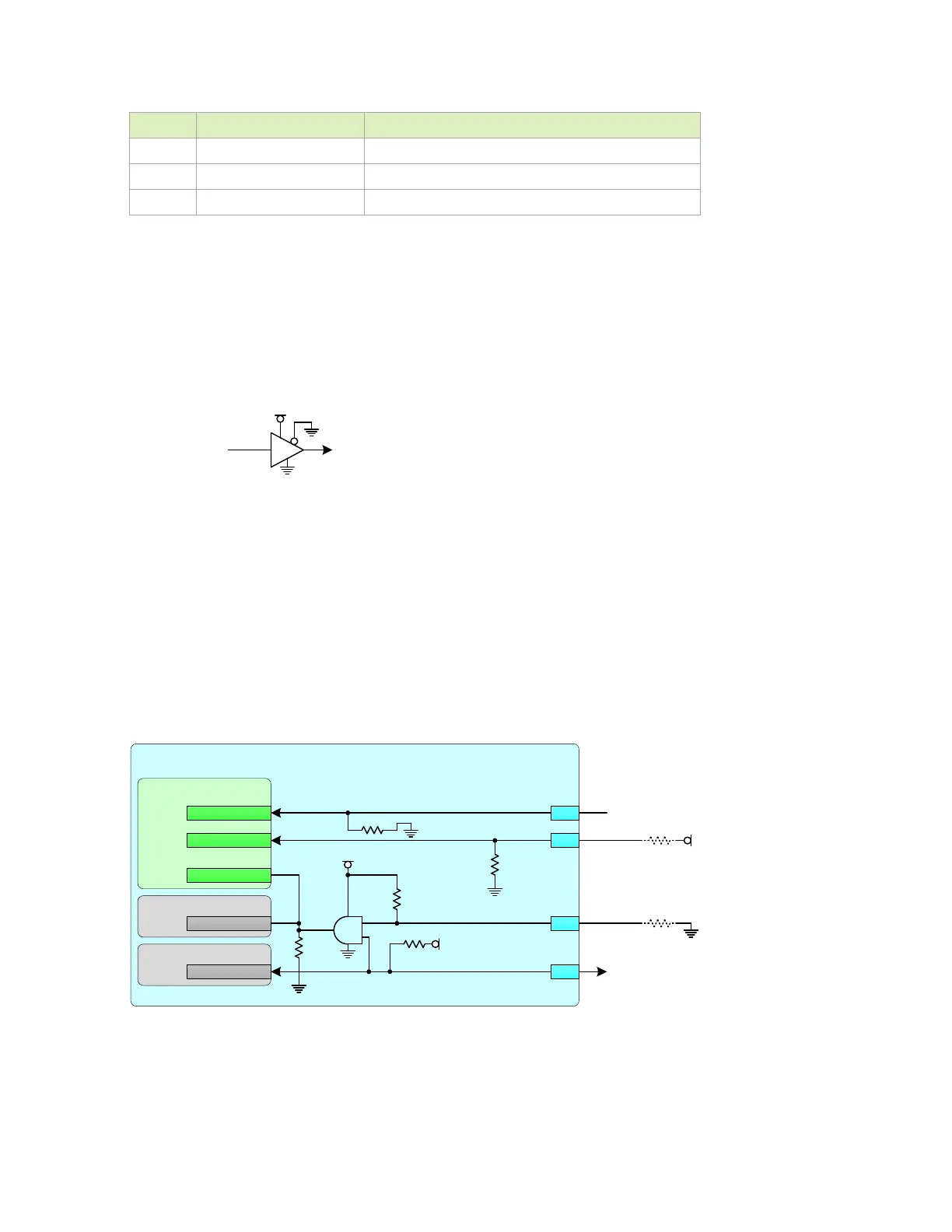
15.4 Boundary Scan Test Mode
To support Boundary Scan Test mode, the SoC NVJTAG_SEL pin must be pulled high and The
SoC must be held in reset without resetting the PMIC. This is done using the
PERIPHERAL_RESET_N pin on the module. The following figure illustrates this. Other
requirements related to supporting boundary scan test mode are described in the
Jetson AGX
Xavier Boundary Scan Requirements and Usage
document.
Figure 15-4. Boundary Scan Connections
Jetson AGX Xavier
PMIC
SoC
Devices requiring sys tem reset
& System Reset Sources
VDD_1V8
R1 - 0 Ω
Leave Resistors R1 & R2 uninstalled
for normal operation. Install both
for boundary scan test mode.
100kΩ
100kΩ
VDDIO_AO_1V8
eMMC
R2 - 0Ω
JTAG_T RST_N
SYS_RESET_N
RESET *
RST I/O
JTAG_T RST_N
L58
PERIPHERAL_RESET_N
L60
SYS_RESET_N
100kΩ
NVJ TA G_ SEL
H59
NVJ TA G_ SEL
TRST on JT AG Conne ct or
G61
100kΩ
VDDIO_AO_1V8
1kΩ

 Loading...


