USB, PCIe, and UFS
Jetson AGX Xavier Series Product DG-09840-001_v2.5 | 46
Parameter Requirement Units Notes
Value: Min/Max 0.075 / 0.2 uF
Only required for TX pair when routed to
connector
Location (max length to adjacent discontinuity) 8 mm
Discontinuity is connector, via, or component
pad
Voiding
GND/PWR void under/above cap
is preferred
Voiding is required if AC cap size is 0603 or
larger
Max Junction capacitance (IO to GND) 0.8 pF e.g. SEMTECH RClamp0524p
Footprint
Pad should be on the net – not
trace stub
Location (max length to adjacent discontinuity) 8 mm
Discontinuity is connector, via, or component
pad
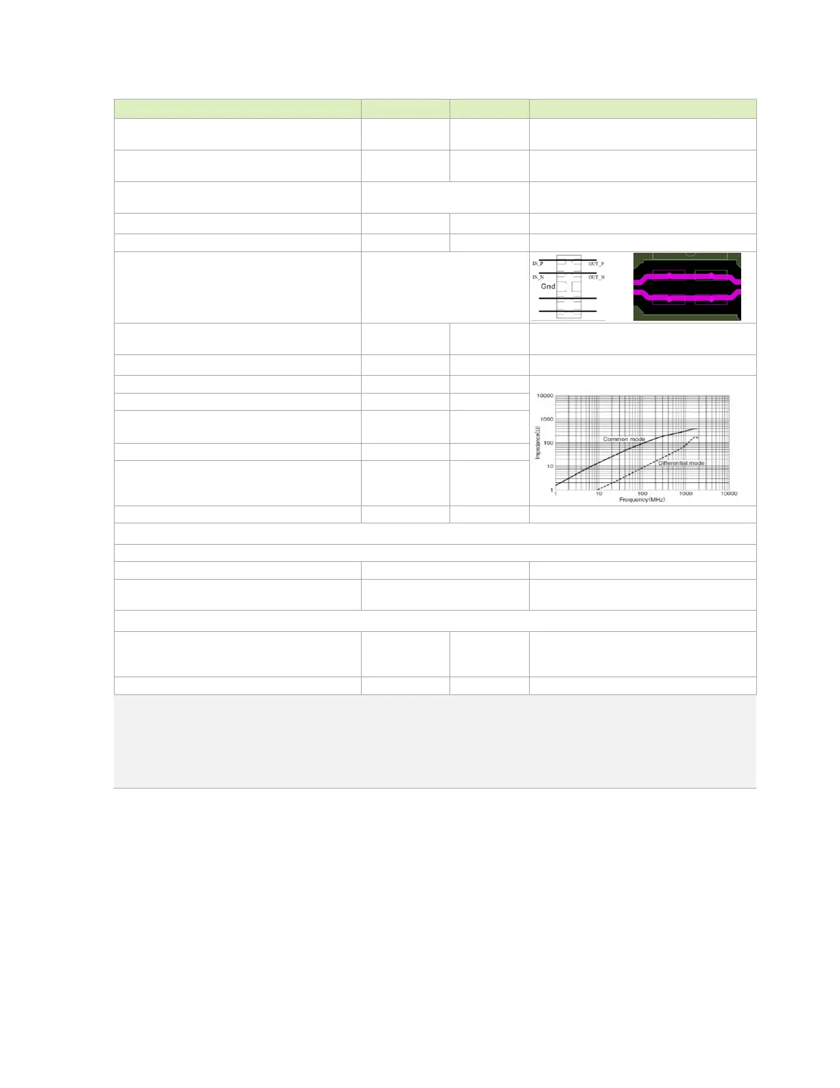
Common-mode impedance @ 100MHz Min/Max 65/90 Ω TDK ACM2012D-900-2P
Max Rdc 0.3 Ω
Differential TDR impedance 90 Ω @TR-200ps
(10%-90%)
Min Sdd21 @ 2.5GHz 2.22 dB
Max Scc21 @ 2.5GHz 19.2 dB
Location 8 mm
FPC (Additional length of Flexible Printed Circuit Board)
The FPC routing should be included for PCB trace calculations (max length, etc.)
Characteristic Impedance Same as PCB
Loss characteristic
Strongly recommend to be same
as PCB or better
If worse than PCB, the PCB and FPC length
must be re-estimated
SMT Connector GND Voiding
GND plane under signal pad should be voided.
Size of void should be the same size as the
pad.
Connector type Connector used must be USB-IF certified
Notes:
1. Up to 4 signal Vias can share a single
return Via
2. Recommend trace length matching to <1ps before Vias or any discontinuity to minimize common mode
conversion.
3. Place
Vias as symmetrically as possible to data pair Vias.
7.1.3 Common USB Routing Guidelines
If routing to USB device or USB connector includes a flex or 2nd PCB, the total routing
including all PCBs and flexes must be used for the max trace and skew calculations.
Keep critical USB related traces away from other signal traces or unrelated power traces and
areas or power supply components.

 Loading...


