Miscellaneous Interfaces
Jetson AGX Xavier Series Product DG-09840-001_v2.5 | 107
13.1.2 De-bounce
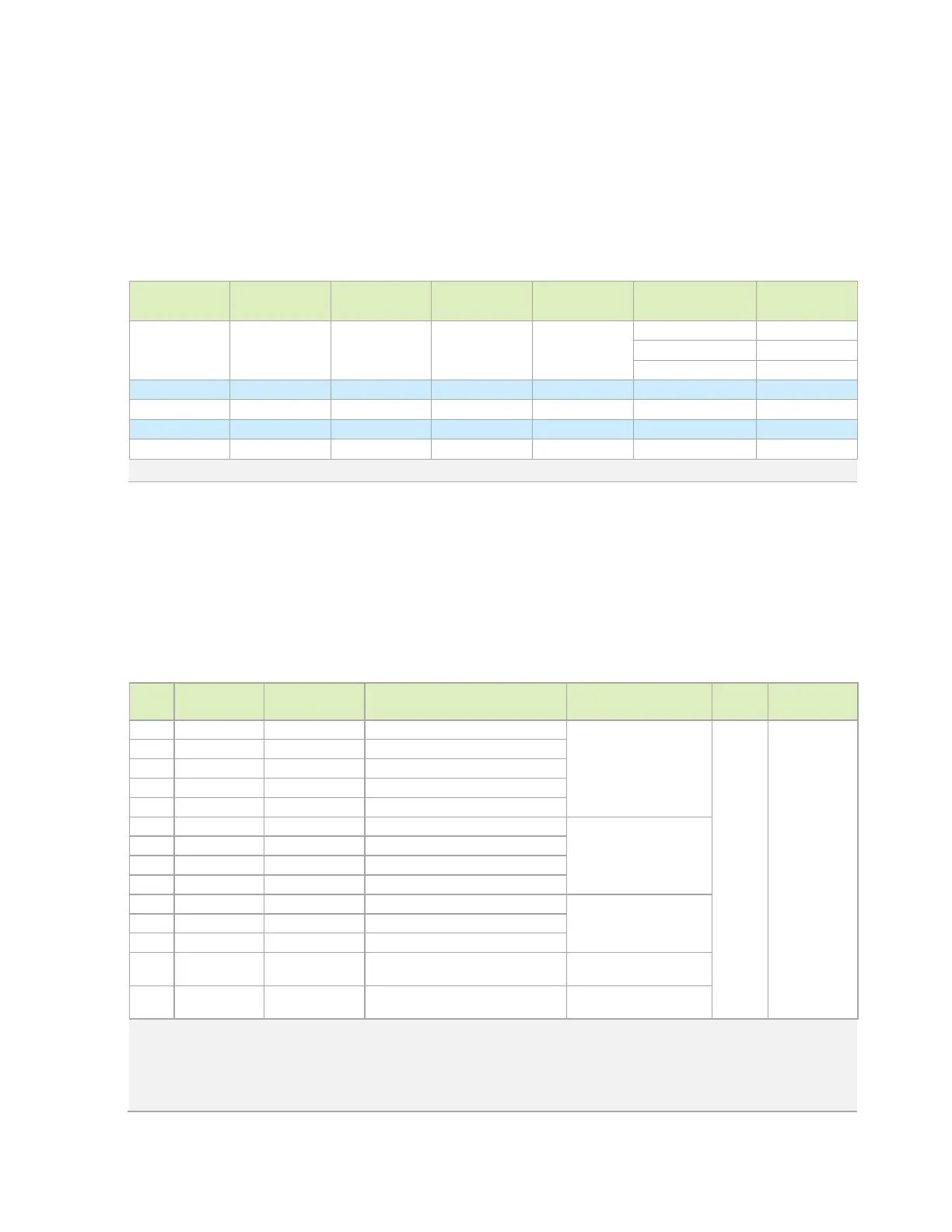
The following table contain the allowable De-bounce settings for the various I2C modes.
Table 13-5. De-bounce Settings – Fast Mode Plus, Fast Mode, and Standard
Mode
I2C Mode
Clock
Source
Source
Clock Freq
I2C Source
Divisor
Sm/Fm
Divisor
De-bounce
Value
I2C SCL
Freq
PLLP_OUT0 408MHz 5 (0x04) 10 (0x9)
0 1016KHz
5:1 905.8KHz
7:6 816KHz
PLLP_OUT0 408MHz 5 (0x4) 26 (0x19) 7:0 392KHz
PLLP_OUT0 408MHz 20 (0x13) 26 (0x19) 7:0 98KHz
Note: sm = standard mode
13.2 SPI
Jetson AGX Xavier brings out three of the SoC SPI interfaces. For JAXi, SPI2 is routed to the
safety MCU if implemented.
Table 13-6. Jetson AGX Xavier SPI Pin Description
Pin #
Module Pin
Name
SoC Signal Usage/Description
Usage on NVIDIA Carrier
Board
Direction
Pin Type
J57 SPI1_CLK SPI1_SCK SPI 1 Clock
Expansion Connector
Bidir CMOS – 1.8V
E55 SPI1_CS0_N SPI1_CS0 SPI 1 Chip Select 0
B56 SPI1_CS1_N SPI1_CS1 SPI 1 Chip Select 1
A56 SPI1_MISO SPI1_MISO SPI 1 Master In / Slave Out
D55 SPI1_MOSI SPI1_MOSI SPI 1 Master Out / Slave In
E61 SPI2_CLK SPI2_SCK SPI 2 Clock (see note 5)
PCIe x16 Connector
D60 SPI2_CS0_N SPI2_CS0 SPI 2 Chip Select 0
D62 SPI2_MISO SPI2_MISO SPI 2 Master In / Slave Out
F60 SPI2_MOSI SPI2_MOSI SPI 2 Master Out / Slave In
F55 SPI3_CLK SPI3_SCK SPI 3 Clock
Not used
C57 SPI3_CS0_N SPI3_CS0 SPI 3 Chip Select 0
D56 SPI3_MISO SPI3_MISO SPI 3 Master In / Slave Out
PCIe x16 Connector
(SLVS_XCLR)
G56 SPI3_MOSI SPI3_MOSI SPI 3 Master Out / Slave In
PCIe x16 Connector
(SLVS_XCE)
Notes:
1. The Direction depends on whether Xavier is the master or slave. If Xavier is master, the clock, chip select and MOSI are outputs and MISO is an
input. If Xavier is slave, the clock, chip select and MOSI are inputs and MISO is an output.
2. In the Type/Dir column, Output is from Jetson AGX Xavier. Input is to Jetson AGX Xavier. Bidir is for Bidirectional signals.
3. JAXi only: SPI2 routed to safety MCU if implemented in design.

 Loading...


