USB, PCIe, and UFS
Jetson AGX Xavier Series Product DG-09840-001_v2.5 | 40
Pin # Module Pin
Name
SoC Signal Usage/Description Usage on NVIDIA
Carrier Board
Direction Pin Type
when Jetson AGX Xavier is Endpoint. Pulled to
3.3V through 47kΩ resistor on-module.
H10 PEX_L5_RST_N PEX_L5_RST_N PCIe 5 Reset. Output when Jetson AGX Xavier is
Root Port. Input when Jetson AGX Xavier is
Endpoint. Pulled to 3.3V through 4.7kΩ resistor
on-module.
Bidir
E31 NVHS0_SLVS_RE
FCLK0_N
NVHS0_REFCLK_
N
PCIe/SLVS Reference Clock 0. Unused if
controller #5 (NVHS[7:0] lanes) configured as
Root Port. Receives 100Mhz clock if configured
as Endpoint.
Input UPHY/SLVS Diff
Pair
E30 NVHS0_SLVS_RE
FCLK0_P
NVHS0_REFCLK_
P
E26 UPHY_
REFCLK1_N
PEX_REFCLK1_N
UPHY Reference Clock 1. Unused. Unused Input UPHY Diff Pair
E27 UPHY_
REFCLK1_P
PEX_REFCLK1_P
F29 UPHY_
PEX_REFCLK2_N
UPHY Reference Clock 2. Unused.
F28 UPHY_
REFCLK2_P
PEX_REFCLK2_P
A8 PEX_WAKE_N PEX_WAKE_N
PCIe Wake. Wake signal shared by all PCIe
interfaces. Pulled to 3.3V through 47kΩ resistor
on-module.
PCIe x16 Connector and
M.2 Key E and
Connector
Input
Open-Drain –
3.3V
Notes:
1. In the Type/Dir column, Output is from Jetson AGX Xavier. Input is to Jetson AGX Xavier. Bidir is for Bidirectional signals.
2. The direction shown in this table for PEX_Lx_RST_N, PEX_Lx_CLKREQ_N and PCIE_WAKE_N signals is true when used for
those PCIe functions. Otherwise if used as GPIOs, the direction is bidirectional.
Table 7-5. UFS and Miscellaneous USB Control Pin Descriptions
Pin # Module Pin Name SoC Signal Usage/Description Usage on NVIDIA Carrier Board Direction Pin Type
A6 UFS0_REF_CLK UFS0_REF_CLK UFS Reference Clock Micro SD / UFS Card Socket Output CMOS – 1.2V
C6 UFS0_RST_N UFS0_RST UFS Reset Micro SD / UFS Card Socket Output CMOS – 1.2V
A62 GPIO10 CAN1_WAKE GPIO USB PD Controller Interrupt Bidir CMOS – 3.3V
F54 GPIO22 USB_VBUS_EN0 GPIO
VDD_5V_SATA Load Switch
Enable
Output CMOS – 1.8V
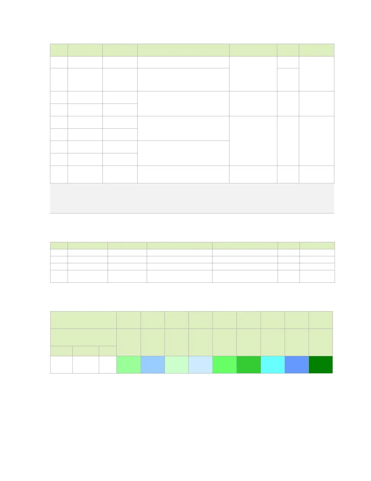
Table 7-6. USB 3.1, PCIe and UFS Lane Mapping Configurations
Jetson AGX Xavier Lanes UPHY0 UPHY1
UPHY[5:2
]
UPHY6 UPHY7
UPHY[9:8
]
UPHY10 UPHY11
NVHS[7:0
]
Avail. Outputs from Jetson
AGX Xavier
USB 3.1 PCIe UFS
3
x4 & 1 x8
1 x1
PCIe x1
(C1)
USB 3.1
(P2)
PCIe x4
(C0)
USB 3.1
(P0)
PCIe x1
(C3)
PCIe x2
(C4)
UFS x1
(0)
USB 3.1
(P3)
PCIe x8
(C5)

 Loading...


