Power
Jetson AGX Xavier Series Product DG-09840-001_v2.5 | 30
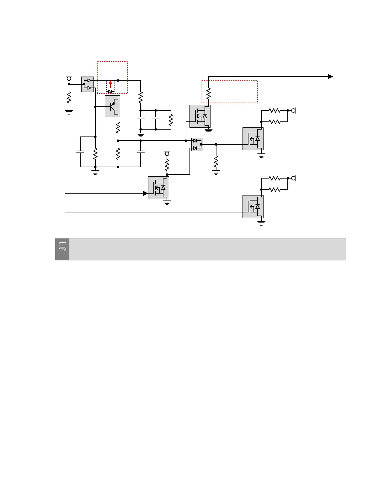
Figure 5-12. Power Discharge
VDD_SRC
10uF
1uF
G
S
D
20 kΩ
10uF
10 kΩ
10 MΩ
0 Ω
20 kΩ, 1%
DISCHARGE
VDDIN_PWR_BAD_N
(Module pin Pin L55)
47 kΩ
VDD_SRC
CARRIER_POWER_ON
(Module pin L62)
BAT54 AWG
BAT54 CW
MMBT
44 03
NT S40 01
NT 1G
NTR4001
NT 1G
E
B
C
G
S
D
1uF
0.05Ω Tol.
10 0kΩ, 1%
10 0k Ω, 1%
G
S
D
VDD_xxx (One for
each c arrier board
sup ply th at needs
to be disc harged)
NT S40 01
NT 1G
G
S
D
NT S40 01
NT 1G
VDD_5V
VI N_ PW R_ ON *
0Ω
0.05Ω Tol.
DV/Dt Droop
Allowance
Tun ing
Disables DV/Dt
circuit if re moved
Note: The resistor values in the discharge circuit for each rail should be tuned to bring the rail
down in the proper timeframe.
5.6 Power and Voltage Monitoring
This section describes the power and voltage monitoring for Jetson AGX Xavier.
5.6.1 Power Loss Detection
The circuit in Figure 5-13 is implemented on the NVIDIA Jetson AGX Xavier carrier board to
detect a loss or unacceptable droop on the main power input (
VCC_SRC).

 Loading...


