USB, PCIe, and UFS
Jetson AGX Xavier Series Product DG-09840-001_v2.5 | 42
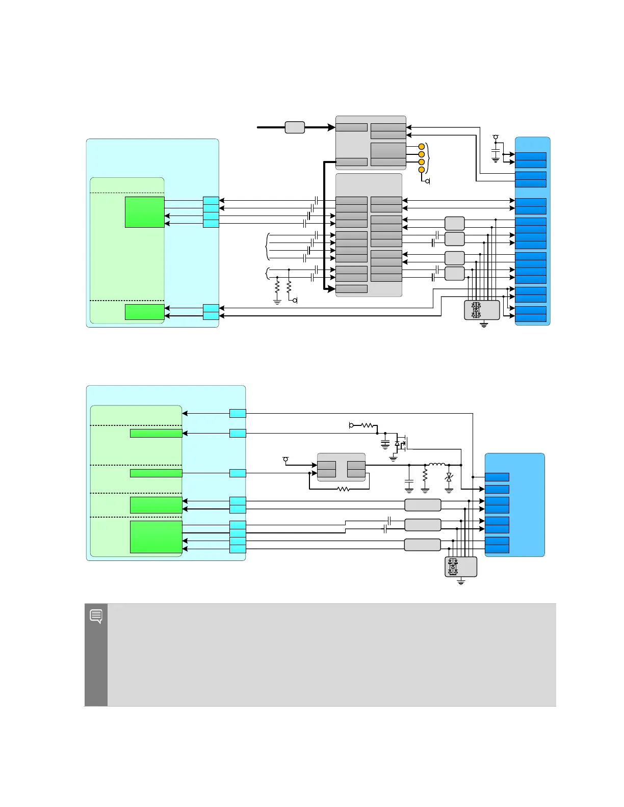
Figure 7-2. Jetson AGX Xavier Carrier Board Design USB Type C
Connection Example
Jetson AGX
Xavier
SoC
USB 2.0
USB0_ DN
USB0_ DP
USB 3.1
PCIe
UFS
VBUS1
F12
F13
PEX_RX1_N
PEX_RX1_P
PEX_TX1_N
PEX_TX1_P
USB Type C Alt
Mode Redriver
Switch
G23
G22
C23
C22
0. 1 uF
0. 1 uF
HDMI_DP0
USB
Type C
VBUS_A
TX1_P
D1_N
D1_P
TX1_N
RX1_P
RX1_N
VBUS_B
CC1
CC2
SBU1
SBU2
TX2_P
TX2_N
RX2_P
RX2_N
D2_N
D2_P
USB0_N
USB0_P
SBU1
SBU2
TX1_P
TX1_N
RX1_P
RX1_N
TX2_P
TX2_N
RX2_P
RX2_N
UPHY_RX1_N
UPHY_RX1_P
U PH Y _T X 1_ N
U PH Y _T X 1_ P
0. 1 uF
0. 1 uF
0. 1 uF
0. 1 uF
CM
Choke
CM
Choke
CM
Choke
CM
Choke
SSTXP
SSTXN
SSRXP
SSRXN
I2C
Module
I2C_GP2
Lev el
Shifter
VDD_3V3VDD_1V8
DP0N/P
E SD
USB PD Controller
CC1 _P1
CC2 _P1
I2C_OUT
I2C_IN
0. 1 uF
0. 1 uF
DP1N/P
DP2N/P
DP3N/P
AUXN
AUXP
DP_AUX_CH0
0. 1 uF
0. 1 uF
0. 1 uF
0. 1 uF
0. 1 uF
0. 1 uF
VDD_3V3
10 0kΩ
10 0kΩ
SW D_ CLK
SW D_ I O
XRES
5V_AO
Te st Poi nts
for Firmware
Programming
Figure 7-3. USB 3.1 USB Micro AB Connection Example
Jetson AGX Xavier
SoC
USB 2.0
USB0_ DP
USB0_ DN
F12
F13
GP IO x
GP IO 10
GP IO 22
USB0_P
USB0_N
UART
USB_VBUS_EN0
F54
USB_VBUS_EN0
Load S witch
EN OC
IN OUT
VDD_5V0
Common
Mode Choke
100kΩ
100Ω
VDD_3V3
G
S
D
10 0Ω
CAN1 _WAKE
x
A62
USB 3.1
Micro AB
VBUS
TX+
D+
D–
TX–
RX+
RX–
ID
USB 3.1
PCIe
UFS
PEX_TX1_P
PEX_TX1_N
PEX_RX1_P
PEX_RX1_N
G23
G22
C23
C22
U PH Y _T X 1_ P
U PH Y _T X 1_ N
UPHY_RX1_P
UPHY_RX1_N
E SD
Common
Mode Choke
0. 1 uF
0. 1 uF
Common
Mode Choke
AO_HV
Notes:
• See the USB.org statement regarding the phasing out of support for the USB 3.x Micro-B and Micro-AB
connector certifications after February 28th, 2021.
• An available GPIO will need to be found to support connections to the ID pin.
• The load switch supplying VBUS should have over current protection. In the figure above this is supported
by routing the over current (OC) pin of the load switch to the GPIO22 (USB_VBUS_EN0) pin which is
bidirectional and can be used to detect an over current condition.

 Loading...


