Display
Jetson AGX Xavier Series Product DG-09840-001_v2.5 | 71
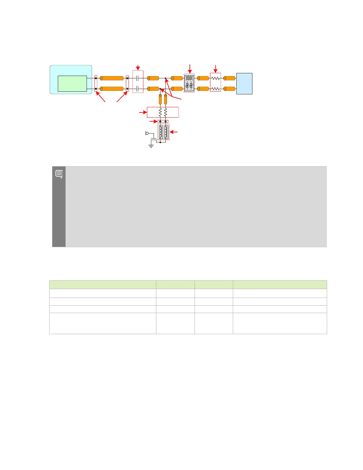
Figure 9-4. HDMI CLK and Data Topology
100Ω*
100Ω*
100Ω*
100Ω*
100Ω*
100Ω*
Module
HDMI
Conn
AC
C AP
Se g D Se g F
3. 3V
49 9Ω,
1%
PCB Vias
PCB Vias
0. 1u F
0. 1u F
R
PD
Com m on Mode
Cho kes & ES D
Se e No te 1
49 9Ω,
1%
Se g B Se g E
Se g C
SoC
95-100Ω 100Ω*
95-100Ω 100Ω*
Main Route
–
Se g A
* Note 3 * Note 3* Note 3 * Note 3
R
S
(See n ote 4)
Choke or Trace
Se e No te 2
Notes:
1. RPD pad must be on the main trace. RPD and ACCAP must be on same layer.
2. Chokes (600 Ω @ 100 MHz) or narrow traces (1 uH@DC-100 MHz) between pull-downs and FET
are required for Standard Technology (through-hole) designs and recommended for HDI
designs.
3. The trace after the main-route via should be routed on the top or bottom layer of the PCB, and
either with 100 ohm differential impedance, or as uncoupled 50 ohm Single Ended traces.
4. RS series resistor is required. See the RS section of Table 9-6 for details.
Table 9-6. HDMI Interface Signal Routing Requirements
Parameter Requirement Units Notes
Max Frequency / UI 5.94 / 168 Gbps / ps Per lane – not total link bandwidth
Topology Point to point Unidirectional, Differential
Termination
At Receiver
On-board
100
500
Ω
Differential To
at receiver
To
near connector

 Loading...


