Miscellaneous Interfaces
Jetson AGX Xavier Series Product DG-09840-001_v2.5 | 106
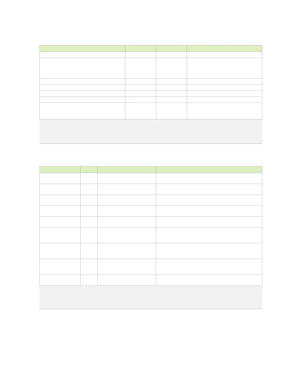
Table 13-3. I2C Interface Signal Routing Requirements
Parameter Requirement Units Notes
Max Frequency - Standard-mode / Fm / Fm+ 100 / 400 / 1000 kHz See Note 1
Topology
Single ended, bi-
directional,
multiple
masters/slaves
Max Loading - Standard-mode / Fm / Fm+ 400 pF Total of all loads
Reference plane
or
Trace Impedance 50 – 60 Ω ±15%
Max Trace Length/Delay
Standard Mode
Fm & Fm+
460 (2890)
220 (1370)
mm (ps)
Notes:
1. Fm = Fast-mode, Fm+ = Fast-mode Plus
2. Avoid routing I2C signals near noisy traces, supplies or components such as a switching power regulator.
3. No requirement for decoupling caps for PWR reference
Table 13-4. I2C Signal Connections
Module Pin Name Type Termination Description
I/OD 1kΩ pull-ups to 1.8V on module
General I2C 1 Clock\Data. Connect to CLK/Data pins of
1.8V devices
I/OD 1kΩ pull-ups to 1.8V on module
General I2C 2 Clock\Data. Connect to CLK/Data pins of
1.8V devices.
I/OD 1kΩ pull-ups to 1.8V on module
General I2C 3 Clock\Data. Connect to CLK/Data pins of
1.8V devices
I/OD 1kΩ pull-ups to 1.8V on module
General I2C 4 Clock\Data. Connect to CLK/Data pins of
1.8V devices.
I/OD 1kΩ pull-ups to 1.8V on module
General I2C 5 Clock\Data. Connect to CLK/Data pins of
1.8V devices.
I/OD
See eDP/HDMI/DP sections for
correct termination
DP_AUX Channel (eDP/DP) or DDC I2C 2 Clock and Data
(HDMI). Connect to AUX_CH_P/N
(DP) or
(HDMI).
Alternately available as I2C IF.
I/OD
See eDP/HDMI/DP sections for
correct termination
DP_AUX Channel (eDP/DP) or DDC I2C 2 Clock and Data
(HDMI). Connect to AUX_CH_P/N
(DP) or
(HDMI).
Alternately available as I2C IF.
I/OD
See eDP/HDMI/DP sections for
correct termination
DP_AUX Channel (eDP/DP) or DDC I2C 2 Clock and Data
(HDMI). Connect to AUX_CH_P/N
(DP) or
(HDMI). Alternately available as I2C IF.
VM_I2C_CLK/DAT
(JAXi only)
I/OD 1kΩ pull-ups to 1.8V on module
Voltage Monitor I2C Clock\Data. Connects to safety MCU
CLK/Data pins if implemented.
Notes:
1. If some devices require a different voltage level than others connected to the same I2C bus, level shifters are required.
2. For I2C interfaces that are pulled up to 1.8V, disable the E_IO_HV option for these pads. For I2C interfaces that are pulled up
to 3.3V, enable the E_IO_HV option. The E_IO_HV option is selected in the Pinmux registers.

 Loading...


