48 Reciter Circuit Description TB8100 Service Manual
© Tait Electronics Limited September 2006
ADC
The I_Q channel triangular analogue waveforms are sampled and
transformed to digits using a 16-bit ADC with a signal-to-noise ratio of
75dB.
FCL Processor and
DAC
The FCL processor runs a DSP-based algorithm which takes the digitised
signals, I_Q and transmit audio, and compares them to the transmit
modulation calibration data.
Using the compared results it attempts to lock FCL_VCXO to the TCXO,
as well as modulate the FCL_VCXO and VCO signals to achieve
modulation flatness across the transmit audio and VCO RF bands.
The FCL processor achieves this by sending the digitised modulation code
through a16-bit DAC. Here the code is translated to analogue signals which
modulate FCL_VCXO and the VCO. The DAC has a signal-to-noise ratio
of 70dB.
2.5.2 Synthesizer
The exciter synthesizer consists of a programmable frequency synthesizer
IC, the exciter VCO, and a modulatable frequency reference.
The synthesizer uses a phase-locked loop to lock the exciter VCO to a
modulatable frequency reference. The synthesizer IC receives the divider
and control information from the RISC processor via a 3-wire serial bus
(clock, data and enable). When the data bits are latched in, the synthesizer
processes the incoming signals from the VCO feedback signal (f
vcofb
) and
the reference oscillator (f
ref
).
The VCO feedback attenuator is a resistive divider that terminates the VCO
feedback signal in a fixed low impedance (50Ω). This attenuates the VCO
RF level down to a level suitable for the RF prescaler (within the synthesizer
IC).
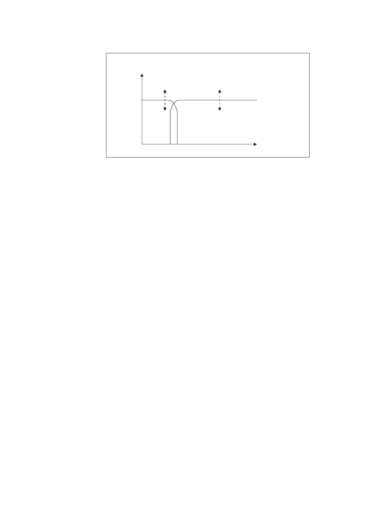
Figure 2.9 Comparison of VCXO and VCO modulation responses
VCXO VCO
150Hz
Gain
Frequency
3kHz
linear relationship
proportianal to the RF
frequency and
FCL_GAIN, measured
during calibration
non-linear relationship,
determined by
CalVcoGain_Corrected,
calculated from the
calibration data
0
 Loading...