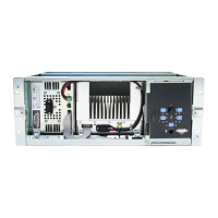
TB8100 Service Manual Reciter Circuit Description 67
© Tait Electronics Limited September 2006
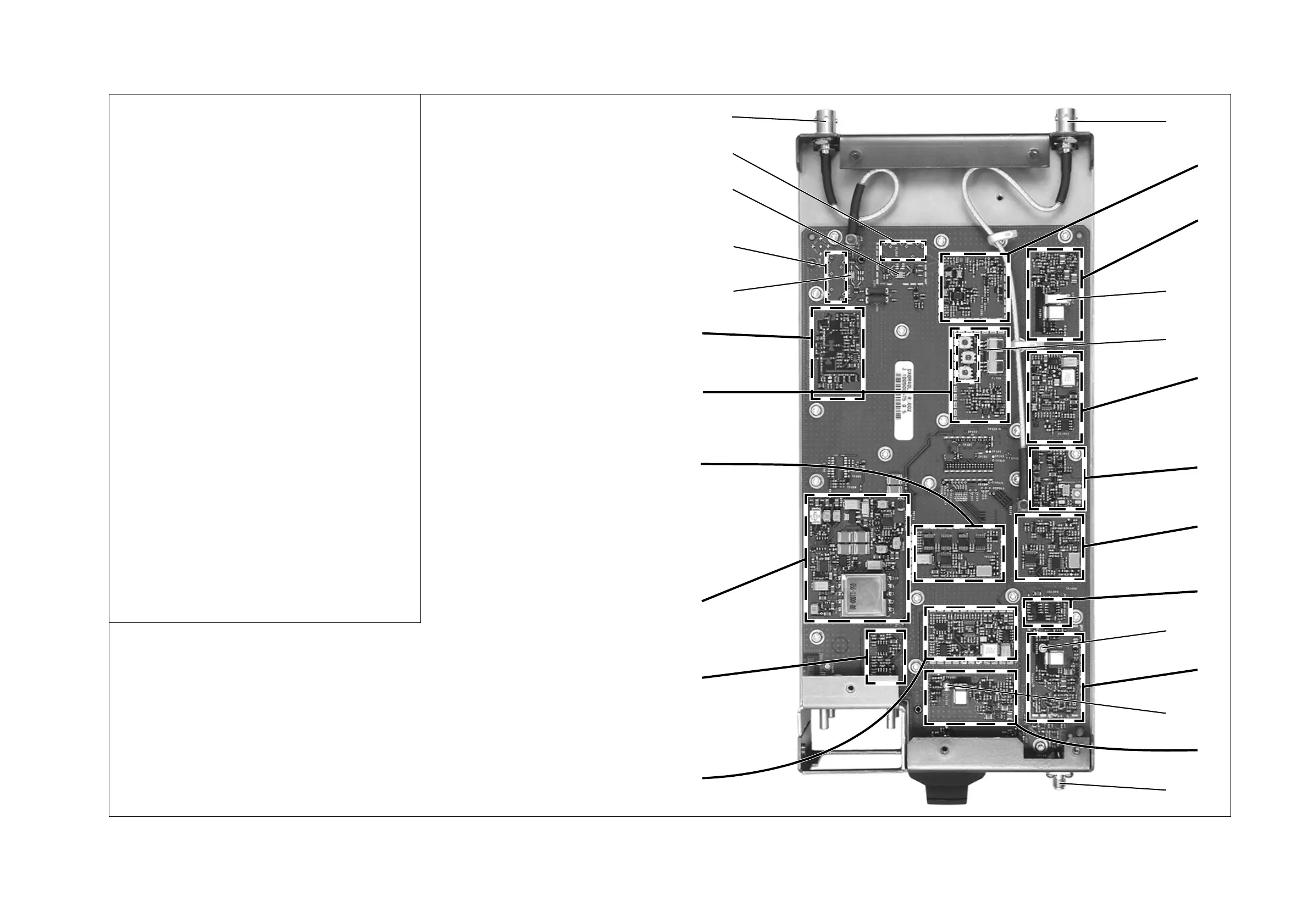
Figure 2.17 Identifying the circuitry on the RF board - K and L bands
b
external reference input
c
mixer and post-mixer buffer
d
receiver VCO
e
receiver VCO trimmer
f
IF tuning elements
g
receiver synthesizer
h
TCXO
i
external reference switch/internal VCXO reference
j
audio buffers
1)
exciter VCO 1 trimmer
1!
exciter VCO 1
1@
exciter VCO 2 trimmer
1#
exciter VCO 2
1$
exciter RF output
1%
exciter synthesizer
1^
FCL buffers
1&
power supply
1*
FCL
1(
IF
2)
front end
2!
SAW filter (L band only)
2@
front end first helicals (K band only)
2#
SAW filter (L band only)
2$
front end second helicals (K band only)
2%
receiver RF input
Note:
In order to show as much of the circuitry as possible in the
photograph, the SMD shields have been removed. The
photograph shows an L-band reciter. The layout of the K-band
reciter circuitry is identical except where noted.
b
c
d
e
f
g
h
1%
1&
1*
1(
2)
2@
2!
2$
i
j
1!
1)
1#
1$
1^
2%
1@
2#
 Loading...