RL78/G1H CHAPTER 14 SERIAL ARRAY UNIT
R01UH0575EJ0120 Rev. 1.20 Page 326 of 920
Dec 22, 2016
14.2 Configuration of Serial Array Unit
The serial array unit includes the following hardware.
Note 1. The lower 8 bits of serial data register mn (SDRmn) can be read or written as the following SFR, depending on the
communication mode.
• CSIp communication ........SIOp (CSIp data register)
• UARTq reception..............RXDq (UARTq receive data register)
• UARTq transmission ........ TXDq (UARTq transmit data register)
Note 2. Output only for SCK20.
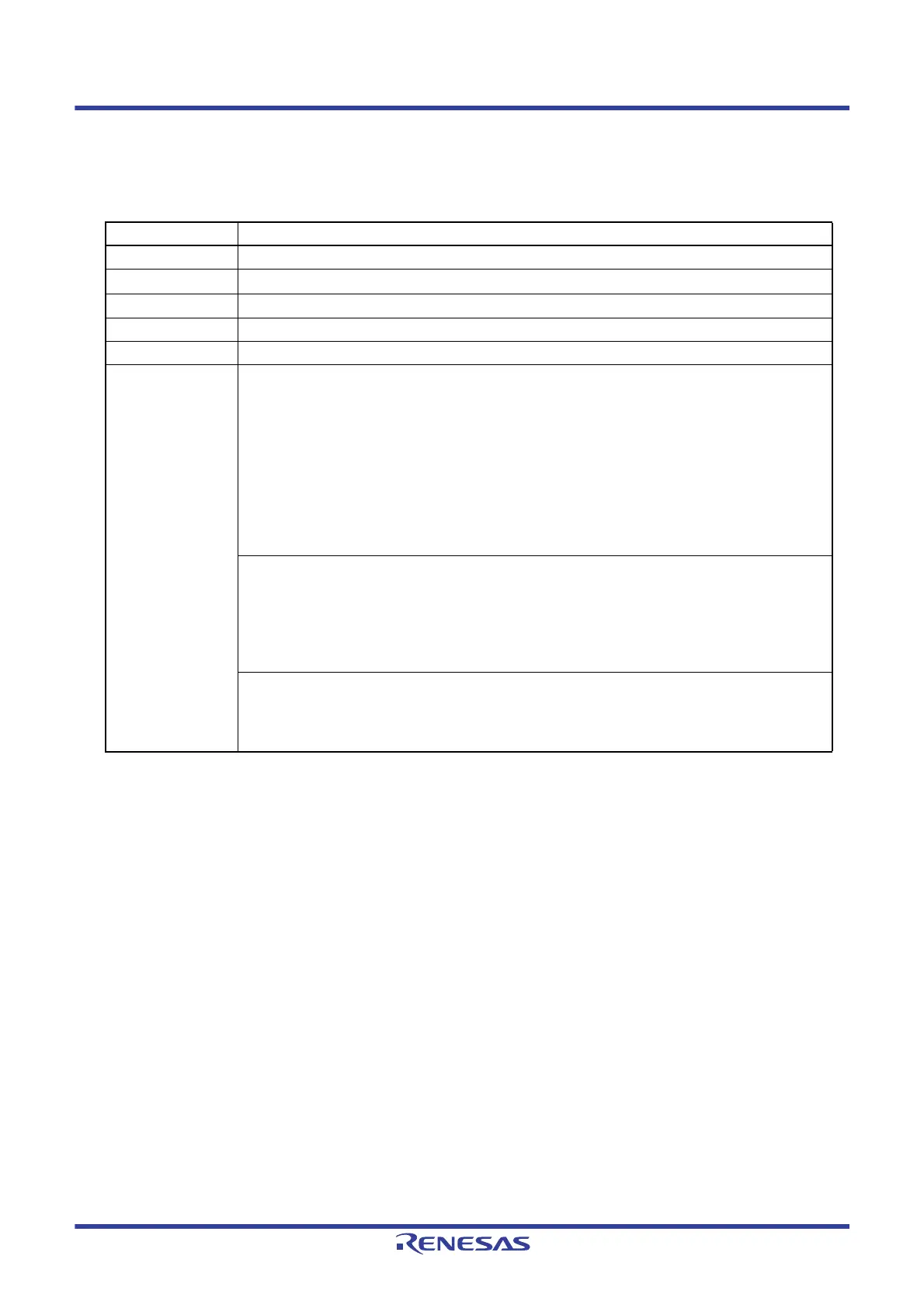
Table 14 - 1 Configuration of Serial Array Unit
Item Configuration
Shift register 8 bits
Buffer register
Lower 8 bits of serial data register mn (SDRmn)
Note 1
Serial clock I/O
SCK10, SCK20, SCK21, SCK30 pins (for 3-wire serial I/O)
Note 2
Serial data input SI10, SI20, SI21, SI30 pins (for 3-wire serial I/O), RxD1, RxD3 pins (for UART)
Serial data output SO10, SO20, SO21, SO30 pins (for 3-wire serial I/O), TxD1, TxD3 pins (for UART)
Control registers <Registers of unit setting block>
• Peripheral enable register 0 (PER0)
• Serial clock select register m (SPSm)
• Serial channel enable status register m (SEm)
• Serial channel start register m (SSm)
• Serial channel stop register m (STm)
• Serial output enable register m (SOEm)
• Serial output register m (SOm)
• Serial output level register m (SOLm)
• Noise filter enable register 0 (NFEN0)
<Registers of each channel>
• Serial data register mn (SDRmn)
• Serial mode register mn (SMRmn)
• Serial communication operation setting register mn (SCRmn)
• Serial status register mn (SSRmn)
• Serial flag clear trigger register mn (SIRmn)
• Port input mode registers 0, 14 (PIM0, PIM14)
• Port output mode registers 0, 14 (POM0, POM14)
• Port mode registers 0, 1, 7, 14 (PM0, PM1, PM7, PM14)
• Port registers 0, 1, 7, 14 (P0, P1, P7, P14)
 Loading...


