RL78/G1H CHAPTER 31 ELECTRICAL SPECIFICATIONS
R01UH0575EJ0120 Rev. 1.20 Page 875 of 920
Dec 22, 2016
31.5 Peripheral Functions Characteristics
AC Timing Test Points
31.5.1 Serial array unit
Note The maximum operating frequencies of the CPU/peripheral hardware clock (fCLK) are:
HS (high-speed main) mode: 32 MHz (2.7 V
≤ VDD ≤ 3.6 V)
16 MHz (2.4 V
≤ VDD ≤ 3.6 V)
LS (low-speed main) mode: 8 MHz (1.8 V
≤ VDD ≤ 3.6 V)
Caution Select the normal input buffer for the RxDq pin and the normal output mode for the TxDq pin by using port input
mode register g (PIMg) and port output mode register g (POMg).
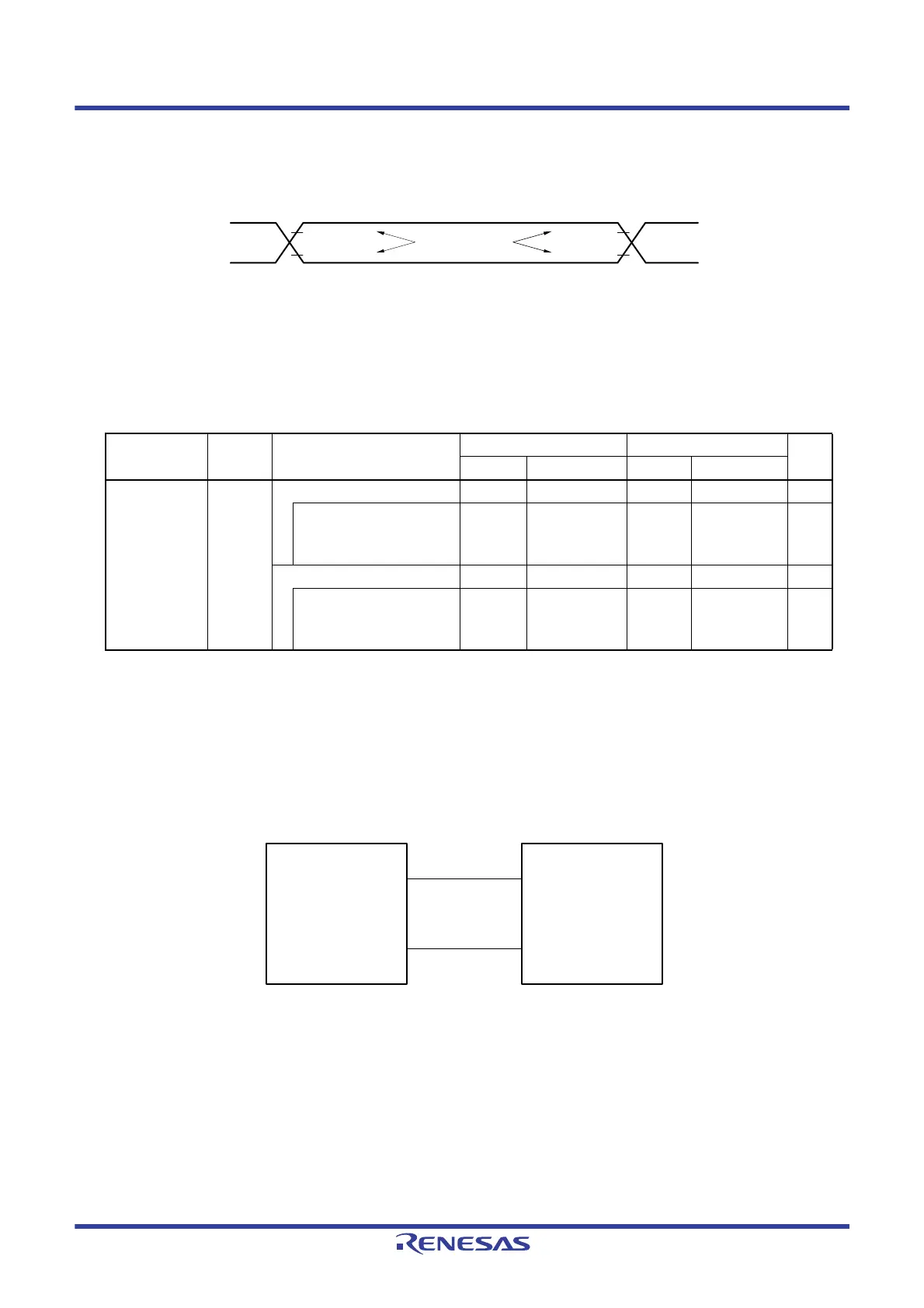
UART mode connection diagram (during communication at same potential)
(1) During communication at same potential (UART mode)
(T
A = ‒40 to +85 °C, 1.8 V ≤ VDD ≤ 3.6 V, VSS = 0 V)
Parameter Symbol Conditions HS (high-speed main) Mode LS (low-speed main) Mode Unit
MIN. MAX. MIN. MAX.
Transfer rate 2.4 V
≤ VDD ≤ 3.6 V fMCK/6 fMCK/6 bps
Theoretical value of the
maximum transfer rate
f
MCK = fCLK
Note
5.3 1.3 Mbps
1.8 V
≤ VDD ≤ 3.6 V fMCK/6 fMCK/6 bps
Theoretical value of the
maximum transfer rate
f
MCK = fCLK
Note
5.3 1.3 Mbps
VIH/VOH
VIL/VOL
VIH/VOH
Test points
V
IL/VOL
RL78 microcontroller
TxDq
RxDq
User’s device
Rx
Tx
 Loading...


