RL78/G1H CHAPTER 31 ELECTRICAL SPECIFICATIONS
R01UH0575EJ0120 Rev. 1.20 Page 891 of 920
Dec 22, 2016
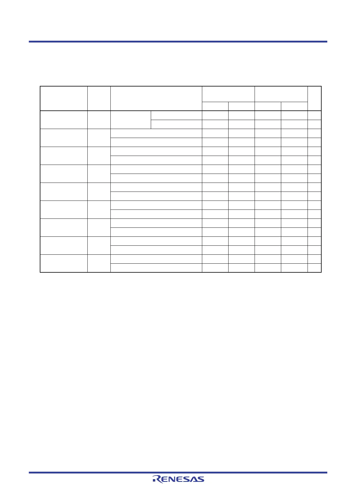
31.5.2 Serial interface IICA
Note 1. The first clock pulse is generated after this period when the start/restart condition is detected.
Note 2. The maximum value (MAX.) of tHD: DAT is during normal transfer and a wait state is inserted in the ACK (acknowledge)
timing.
Remark The maximum value of Cb (communication line capacitance) and the value of Rb (communication line pull-up resistor) at
that time in each mode are as follows.
Standard mode: C
b = 400 pF, Rb = 2.7 kΩ
(1) I
2
C standard mode
(T
A = ‒40 to +85 °C, 1.8 V ≤ VDD ≤ 3.6 V, VSS = 0 V)
Parameter Symbol Conditions HS (high-speed main)
mode
LS (low-speed main)
mode
Unit
MIN. MAX. MIN. MAX.
SCLA0 clock
frequency
f
SCL Standard mode:
f
CLK ≥ 1 MHz
2.7 V
≤ VDD ≤ 3.6 V 0 100 0 100 kHz
1.8 V
≤ VDD ≤ 3.6 V 0 100 0 100 kHz
Setup time of restart
condition
t
SU: STA 2.7 V ≤ VDD ≤ 3.6 V 4.7 4.7 μs
1.8 V
≤ VDD ≤ 3.6 V 4.7 4.7 μs
Hold time
Note 1
tHD: STA 2.7 V ≤ VDD ≤ 3.6 V 4.0 4.0 μs
1.8 V
≤ VDD ≤ 3.6 V 4.0 4.0 μs
Hold time when
SCLA0 = “L”
t
LOW 2.7 V ≤ VDD ≤ 3.6 V 4.7 4.7 μs
1.8 V
≤ VDD ≤ 3.6 V 4.7 4.7 μs
Hold time when
SCLA0 = “H”
t
HIGH 2.7 V ≤ VDD ≤ 3.6 V 4.0 4.0 μs
1.8 V
≤ VDD ≤ 3.6 V 4.0 4.0 μs
Data setup time
(reception)
t
SU: DAT 2.7 V ≤ VDD ≤ 3.6 V 250 250 ns
1.8 V
≤ VDD ≤ 3.6 V 250 250 ns
Data hold time
(transmission)
Note 2
tHD: DAT 2.7 V ≤ VDD ≤ 3.6 V 0 3.45 0 3.45 μs
1.8 V
≤ VDD ≤ 3.6 V 0 3.45 0 3.45 μs
Setup time of stop
condition
t
SU: STO 2.7 V ≤ VDD ≤ 3.6 V 4.0 4.0 μs
1.8 V
≤ VDD ≤ 3.6 V 4.0 4.0 μs
Bus-free time t
BUF 2.7 V ≤ VDD ≤ 3.6 V 4.7 4.7 μs
1.8 V
≤ VDD ≤ 3.6 V 4.7 4.7 μs
 Loading...


