RL78/G1H CHAPTER 31 ELECTRICAL SPECIFICATIONS
R01UH0575EJ0120 Rev. 1.20 Page 860 of 920
Dec 22, 2016
31.3 DC Characteristics
31.3.1 Pin characteristics
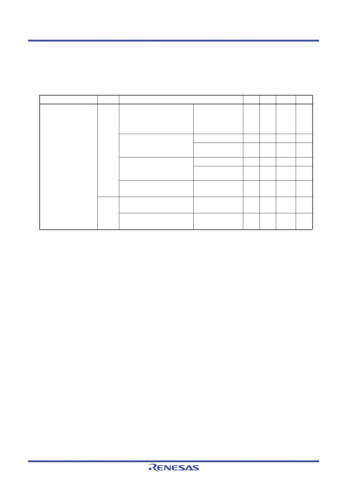
Note 1. Value of current at which the device operation is guaranteed even if the current flows from the VDD pin to an output pin.
Note 2. Do not exceed the total current value.
Note 3. Specification under conditions where the duty factor ≤ 70%.
The output current value that has changed to the duty factor > 70% the duty ratio can be calculated with the following
expression (when changing the duty factor from 70% to n%).
• Total output current of pins = (I
OH × 0.7)/(n × 0.01)
<Example> Where n = 80% and I
OH = ‒10.0 mA
Total output current of pins = (‒10.0 × 0.7)/(80 × 0.01) ≈ ‒8.7 mA
However, the current that is allowed to flow into one pin does not vary depending on the duty factor.
A current higher than the absolute maximum rating must not flow into one pin.
Note 4. ‒100 mA for industrial applications (R5F11FxxDxx).
Caution P02 to P04, P71, P80 to P82, and P142 to P144 do not output high level in N-ch open-drain mode.
Remark Unless specified otherwise, the characteristics of alternate-function pins are the same as those of the port pins.
(TA = ‒40 to +85 °C, 1.8 V ≤ VDD ≤ 3.6 V, VSS = 0 V)
Items Symbol Conditions MIN. TYP. MAX. Unit
Output current, high
Note 1
IOH1 Per pin for P02 to P04, P31,
P40, P70 to P72, P75 to P77,
P80 to P82, P100, P120, P130,
P140 to P144
‒10.0
Note 2
mA
Total of P02 to P04, P40, P120,
P130, P140 to P144
(When duty ≤ 70%
Note 3
)
2.7 V ≤ V
DD ≤ 3.6 V ‒10.0 mA
1.8 V ≤ V
DD < 2.7 V
‒5.0 mA
Total of P31, P70 to P72,
P75 to P77, P80 to P82, P100
(When duty ≤ 70%
Note 3
)
2.7 V ≤ V
DD ≤ 3.6 V ‒19.0 mA
1.8 V ≤ V
DD < 2.7 V
‒10.0 mA
Total of all pins
(When duty ≤ 70%
Note 3
)
‒29.0
Note 4
mA
I
OH2 Per pin for P20 to P22, P155,
P156
‒0.1
Note 2
mA
Total of all pins
(When duty ≤ 70%
Note 3
)
‒0.5 mA
 Loading...


